- 您現(xiàn)在的位置:買賣IC網(wǎng) > PDF目錄377919 > MB90F548GPF (FUJITSU LTD) 16-bit Proprietary Microcontroller PDF資料下載
參數(shù)資料
| 型號: | MB90F548GPF |
| 廠商: | FUJITSU LTD |
| 元件分類: | 微控制器/微處理器 |
| 英文描述: | 16-bit Proprietary Microcontroller |
| 中文描述: | 16-BIT, FLASH, 16 MHz, MICROCONTROLLER, PQFP100 |
| 封裝: | 14 X 20 MM, 3.35 MM HEIGHT, 0.65 MM PITCH, PLASTIC, QFP-100 |
| 文件頁數(shù): | 52/67頁 |
| 文件大小: | 746K |
| 代理商: | MB90F548GPF |
第1頁第2頁第3頁第4頁第5頁第6頁第7頁第8頁第9頁第10頁第11頁第12頁第13頁第14頁第15頁第16頁第17頁第18頁第19頁第20頁第21頁第22頁第23頁第24頁第25頁第26頁第27頁第28頁第29頁第30頁第31頁第32頁第33頁第34頁第35頁第36頁第37頁第38頁第39頁第40頁第41頁第42頁第43頁第44頁第45頁第46頁第47頁第48頁第49頁第50頁第51頁當前第52頁第53頁第54頁第55頁第56頁第57頁第58頁第59頁第60頁第61頁第62頁第63頁第64頁第65頁第66頁第67頁
MB90540/540G/545/545G Series
52
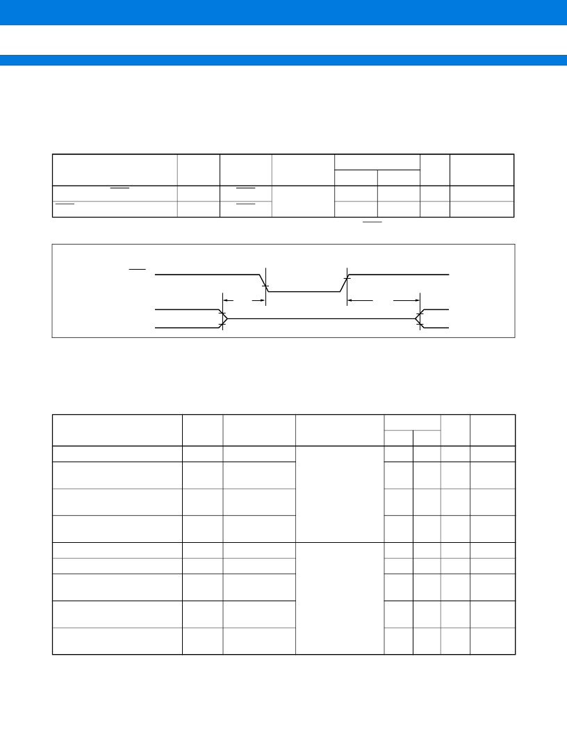
(8) Hold Timing
(MB90F543/F549 : V
CC
=
4.5 V to 5.5 V, V
SS
=
0.0 V, T
A
=
40
°
C to
+
85
°
C)
(MB90543G(S)/547G(S)/548G(S)/F548GL(S): V
CC
=
3.5 V to 5.5 V, V
SS
=
AV
SS
=
0.0 V, T
A
=
40
°
C to
+
105
°
C)
(Other than MB90F543/F549/543G(S)/547G(S)/548G(S)/F548GL(S):
V
CC
=
5.0 V
±
10
%
, V
SS
=
AV
SS
=
0.0 V, T
A
=
40
°
C to
+
105
°
C)
Note : There is more than 1 cycle from the time HRQ is read to the time the HAK is changed.
(9) UART0/1, Serial I/O Timing
(MB90F543/F549 : V
CC
=
4.5 V to 5.5 V, V
SS
=
0.0 V, T
A
=
40
°
C to
+
85
°
C)
(MB90543G(S)/547G(S)/548G(S)/F548GL(S): V
CC
=
3.5 V to 5.5 V, V
SS
=
AV
SS
=
0.0 V, T
A
=
40
°
C to
+
105
°
C)
(Other than MB90F543/F549/543G(S)/547G(S)/548G(S)/F548GL(S):
V
CC
=
5.0 V
±
10
%
, V
SS
=
AV
SS
=
0.0 V, T
A
=
40
°
C to
+
105
°
C)
Note :
AC characteristic in CLK synchronized mode.
C
L
is load capacity value of pins when testing.
For t
CP
(Machine clock cycle time) , refer to “ (1) Clock Timing”.
Parameter
Symbol
Pin name
Condition
Value
Units
Remarks
Min
Max
Pin floating
→
HAK
↓
time
HAK
↑
time
→
Pin valid time
t
XHAL
HAK
30
t
CP
ns
t
HAHV
HAK
t
CP
2 t
CP
ns
Parameter
Symbol
Pin name
Condition
Value
Units Remarks
Min
Max
Serial clock cycle time
t
SCYC
SCK0 to SCK2
Internal clock opera-
tion output pins are
C
L
=
80 pF
+
1 TTL.
8 t
CP
ns
SCK
↓→
SOT delay time
t
SLOV
SCK0 to SCK2,
SOT0 to SOT2
80
80
ns
Valid SIN
→
SCK
↑
t
IVSH
SCK0 to SCK2,
SIN0 to SIN2
100
ns
SCK
↑→
Valid SIN hold time
t
SHIX
SCK0 to SCK2,
SIN0 to SIN2
60
ns
Serial clock “H” pulse width
t
SHSL
SCK0 to SCK2
External clock oper-
ation output pins are
C
L
=
80 pF
+
1 TTL.
4 t
CP
ns
Serial clock “L” pulse width
t
SLSH
SCK0 to SCK2
4 t
CP
ns
SCK
↓→
SOT delay time
t
SLOV
SCK0 to SCK2,
SOT0 to SOT2
150
ns
Valid SIN
→
SCK
↑
t
IVSH
SCK0 to SCK2,
SIN0 to SIN2
60
ns
SCK
↑→
Valid SIN hold time
t
SHIX
SCK0 to SCK2,
SIN0 to SIN2
60
ns
HAK
t
XHAL
t
HAHV
2.4 V
0.8 V
2.4 V
0.8 V
2.4 V
0.8 V
Each pin
High impedance
Hold Timing
相關(guān)PDF資料 |
PDF描述 |
|---|---|
| MB90F548GPFV | 16-bit Proprietary Microcontroller |
| MB90F546GSPF | CONNECTOR ACCESSORY |
| MB90F546GSPFV | CONNECTOR ACCESSORY |
| MB90F548GSPF | 16-bit Proprietary Microcontroller |
| MB90540G | 16-bit Proprietary Microcontroller |
相關(guān)代理商/技術(shù)參數(shù) |
參數(shù)描述 |
|---|---|
| MB90F548GPFR-GSE1 | 制造商:FUJITSU 功能描述: |
| MB90F548GSPFR-GE1 | 制造商:FUJITSU 功能描述: |
| MB90F549PFR-GE1 | 制造商:FUJITSU 功能描述: |
| MB90F562BPMC-GE1 | 制造商:FUJITSU 功能描述: |
| MB90F562PMCR-GE1 | 制造商:FUJITSU 功能描述: |
發(fā)布緊急采購,3分鐘左右您將得到回復。