- 您現(xiàn)在的位置:買賣IC網(wǎng) > PDF目錄201871 > MB90F548GLSPF 16-BIT, FLASH, 16 MHz, MICROCONTROLLER, PQFP100 PDF資料下載
參數(shù)資料
| 型號: | MB90F548GLSPF |
| 元件分類: | 微控制器/微處理器 |
| 英文描述: | 16-BIT, FLASH, 16 MHz, MICROCONTROLLER, PQFP100 |
| 封裝: | PLASTIC, QFP-100 |
| 文件頁數(shù): | 9/67頁 |
| 文件大?。?/td> | 746K |
| 代理商: | MB90F548GLSPF |
第1頁第2頁第3頁第4頁第5頁第6頁第7頁第8頁當(dāng)前第9頁第10頁第11頁第12頁第13頁第14頁第15頁第16頁第17頁第18頁第19頁第20頁第21頁第22頁第23頁第24頁第25頁第26頁第27頁第28頁第29頁第30頁第31頁第32頁第33頁第34頁第35頁第36頁第37頁第38頁第39頁第40頁第41頁第42頁第43頁第44頁第45頁第46頁第47頁第48頁第49頁第50頁第51頁第52頁第53頁第54頁第55頁第56頁第57頁第58頁第59頁第60頁第61頁第62頁第63頁第64頁第65頁第66頁第67頁
MB90540/540G/545/545G Series
17
s
s HANDLING DEVICES
(1) Preventing latch-up
CMOS IC chips may suffer latch-up under the following conditions :
A voltage higher than VCC or lower than VSS is applied to an input or output pin.
A voltage higher than the rated voltage is applied between VCC and VSS.
The AVcc power supply is applied before the VCC voltage.
Latch-up may increase the power supply current drastically, causing thermal damage to the device.
For the same reason, care must also be taken in not allowing the analog power-supply voltage (AVCC, AVRH) to
exceed the digital power-supply voltage.
(2) Handling unused pins
Leaving unused input pins open may result in misbehavior or latch up and possible permanent damage of the
device. Therefor they must be pulled up or pulled down through resistors. In this case those resistors should be
more than 2 k
.
Unused bi-directional pins should be set to the output state and can be left open, or the input state with the
above described connection.
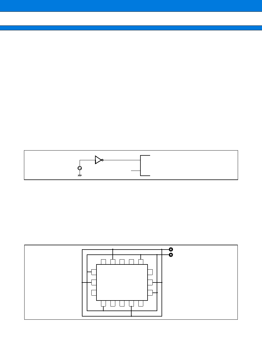
(3) Using external clock
To use external clock, drive X0 pin only and leave X1 pin unconnected.
Below is a diagram of how to use external clock.
(4) Use of the sub-clock
Use one clock system parts when the sub-clock is not used. In that case, pull-down the pin X0A and leave the
pin X1A open. When using two clock system parts, a 32 kHz oscillator has to be connected to the X0A and X1A
pins.
(5) Power supply pins (VCC/VSS)
In products with multiple VCC or VSS pins, the pins of a same potential are internally connected in the device to
avoid abnormal operations including latch-up. However you must connect the pins to an external power and a
ground line to lower the electro-magnetic emission level to prevent abnormal operation of strobe signals caused
by the rise in the ground level, and to conform to the total current rating.
Make sure to connect VCC and VSS pins via the lowest impedance to power lines.
It is recommended to provide a bypass capacitor of around 0.1
F between VCC and VSS pins near the device.
X0
X1
MB90540/545 Series
Open
VCC
VSS
MB90540/545
Series
相關(guān)PDF資料 |
PDF描述 |
|---|---|
| M3727GM6-XXXSP | 8-BIT, MROM, 8.1 MHz, MICROCONTROLLER, PDIP42 |
| M32180F8VFP | 32-BIT, FLASH, 64 MHz, RISC MICROCONTROLLER, PQFP240 |
| M34280E1GP | 4-BIT, OTPROM, 4 MHz, MICROCONTROLLER, PDSO20 |
| M34280M1-XXXFP | 4-BIT, MROM, 4 MHz, MICROCONTROLLER, PDSO20 |
| M34280M1-XXXGP | 4-BIT, MROM, 4 MHz, MICROCONTROLLER, PDSO20 |
相關(guān)代理商/技術(shù)參數(shù) |
參數(shù)描述 |
|---|---|
| MB90F548GPFR-GSE1 | 制造商:FUJITSU 功能描述: |
| MB90F548GSPFR-GE1 | 制造商:FUJITSU 功能描述: |
| MB90F549PFR-GE1 | 制造商:FUJITSU 功能描述: |
| MB90F562BPMC-GE1 | 制造商:FUJITSU 功能描述: |
| MB90F562PMCR-GE1 | 制造商:FUJITSU 功能描述: |
發(fā)布緊急采購,3分鐘左右您將得到回復(fù)。