- 您現(xiàn)在的位置:買賣IC網(wǎng) > PDF目錄377925 > MB90F367ES (Fujitsu Limited) 16-bit Proprietary Microcontroller PDF資料下載
參數(shù)資料
| 型號(hào): | MB90F367ES |
| 廠商: | Fujitsu Limited |
| 英文描述: | 16-bit Proprietary Microcontroller |
| 中文描述: | 16位微控制器專有 |
| 文件頁數(shù): | 7/60頁 |
| 文件大小: | 676K |
| 代理商: | MB90F367ES |
第1頁第2頁第3頁第4頁第5頁第6頁當(dāng)前第7頁第8頁第9頁第10頁第11頁第12頁第13頁第14頁第15頁第16頁第17頁第18頁第19頁第20頁第21頁第22頁第23頁第24頁第25頁第26頁第27頁第28頁第29頁第30頁第31頁第32頁第33頁第34頁第35頁第36頁第37頁第38頁第39頁第40頁第41頁第42頁第43頁第44頁第45頁第46頁第47頁第48頁第49頁第50頁第51頁第52頁第53頁第54頁第55頁第56頁第57頁第58頁第59頁第60頁
MB90360E Series
7
■
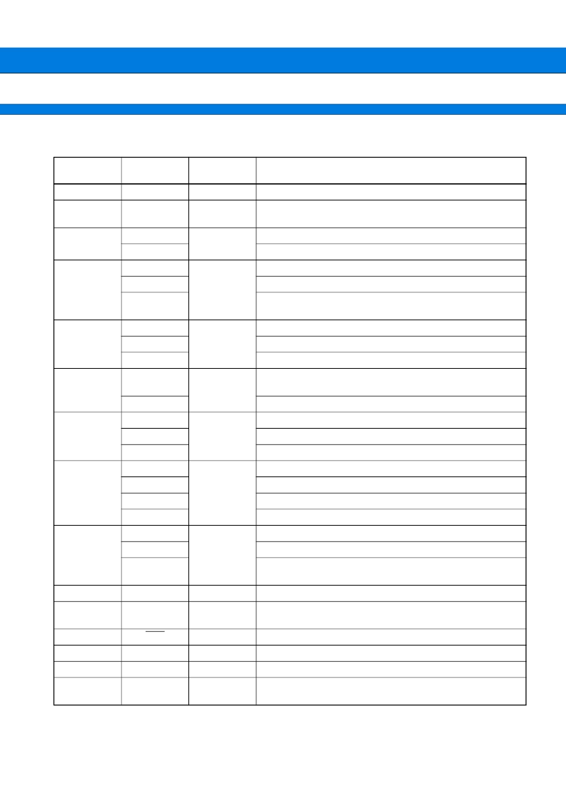
PIN DESCRIPTION
(Continued)
Pin No.
Pin name
I/O circuit
type*
Function
1
AV
CC
I
V
CC
power input pin for analog circuit.
Power (Vref
+
) input pin for A/D converter.
It should be below V
CC
.
2
AVR
3 to 8
P60 to P65
H
General-purpose I/O port.
AN0 to AN5
Analog input pins for A/D converter.
9, 10
P66, P67
H
General-purpose I/O port.
AN6, AN7
Analog input pins for A/D converter.
PPGC (D) ,
PPGE (F)
Output pins for PPG.
11
P80
F
General-purpose I/O port.
ADTG
Trigger input pin for A/D converter.
INT12R
External interrupt request input pin for INT12.
12 to 14
P50 to P52
H
General-purpose I/O port (P50 has different I/O circuit type from
MB90V340E) .
AN8 to AN10
Analog input pins for A/D converter.
15
P53
H
General-purpose I/O port.
AN11
Analog input pin for A/D converter.
TIN3
Event input pin for reload timer 3.
16
P54
H
General-purpose I/O port.
AN12
Analog input pin for A/D converter.
TOT3
Output pin for reload timer 3
INT8
External interrupt request input pin for INT8.
17 to 19
P55 to P57
H
General-purpose I/O port.
AN13 to AN15
Analog input pins for A/D converter.
INT10, INT11,
INT13
External interrupt request input pins for INT10, INT11, INT13.
20
MD2
D
Input pin for operation mode specification.
21, 22
MD1,
MD0
C
Input pins for operation mode specification.
23
RST
E
Reset input pin.
24
V
CC
Power input pin (3.5 V to 5.5 V) .
25
V
SS
Power input pin (0 V) .
26
C
I
Power supply stabilization capacitor pin. It should be connected
to a higher than or equal to 0.1
μ
F ceramic condenser.
相關(guān)PDF資料 |
PDF描述 |
|---|---|
| MB90F367ESPMT | 16-bit Proprietary Microcontroller |
| MB90F367TE | 16-bit Proprietary Microcontroller |
| MB90F367TEPMT | 16-bit Proprietary Microcontroller |
| MB90F367TES | 16-bit Proprietary Microcontroller |
| MB90F367TESPMT | 16-bit Proprietary Microcontroller |
相關(guān)代理商/技術(shù)參數(shù) |
參數(shù)描述 |
|---|---|
| MB90F367TPMCR-GE1 | 制造商:FUJITSU 功能描述: |
| MB90F367TPMCR-G-JNE1 | 制造商:FUJITSU 功能描述: |
| MB90F367TPMCR-GSE1 | 制造商:FUJITSU 功能描述: |
| MB90F367TSPMCR-GE1 | 制造商:FUJITSU 功能描述: |
| MB90F367TSPMCR-GSE1 | 制造商:FUJITSU 功能描述: |
發(fā)布緊急采購,3分鐘左右您將得到回復(fù)。