- 您現(xiàn)在的位置:買賣IC網(wǎng) > PDF目錄377925 > MB90F362TPMT (Fujitsu Limited) 16-bit Proprietary Microcontroller PDF資料下載
參數(shù)資料
| 型號(hào): | MB90F362TPMT |
| 廠商: | Fujitsu Limited |
| 英文描述: | 16-bit Proprietary Microcontroller |
| 中文描述: | 16位微控制器專有 |
| 文件頁(yè)數(shù): | 56/59頁(yè) |
| 文件大小: | 262K |
| 代理商: | MB90F362TPMT |
第1頁(yè)第2頁(yè)第3頁(yè)第4頁(yè)第5頁(yè)第6頁(yè)第7頁(yè)第8頁(yè)第9頁(yè)第10頁(yè)第11頁(yè)第12頁(yè)第13頁(yè)第14頁(yè)第15頁(yè)第16頁(yè)第17頁(yè)第18頁(yè)第19頁(yè)第20頁(yè)第21頁(yè)第22頁(yè)第23頁(yè)第24頁(yè)第25頁(yè)第26頁(yè)第27頁(yè)第28頁(yè)第29頁(yè)第30頁(yè)第31頁(yè)第32頁(yè)第33頁(yè)第34頁(yè)第35頁(yè)第36頁(yè)第37頁(yè)第38頁(yè)第39頁(yè)第40頁(yè)第41頁(yè)第42頁(yè)第43頁(yè)第44頁(yè)第45頁(yè)第46頁(yè)第47頁(yè)第48頁(yè)第49頁(yè)第50頁(yè)第51頁(yè)第52頁(yè)第53頁(yè)第54頁(yè)第55頁(yè)當(dāng)前第56頁(yè)第57頁(yè)第58頁(yè)第59頁(yè)
MB90360 Series
56
7.
Notes on A/D Converter Section
Use the device with external circuits of the following output impedance for analog inputs :
Recommended output impedance of external circuits are : Approx. 1.5 k
or lower (4.0 V
≤
AV
CC
≤
5.5 V,
sampling period
=
0.5
μ
s)
If an external capacitor is used, in consideration of the effect by tap capacitance caused by external capacitors
and on-chip capacitors, capacitance of the external one is recommended to be several thousand times as
high as internal capacitor.
If output impedance of an external circuit is too high, a sampling period for an analog voltage may be
insufficient.
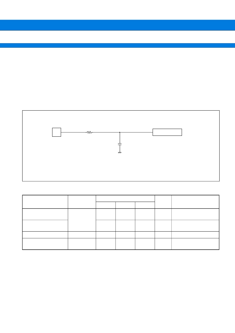
Analog input circuit model
8.
Flash Memory Program/Erase Characteristics
* : This value comes from the technology qualification (using Arrhenius equation to translate high temperature
measurements into normalized value at
+
85
°
C) .
Parameter
Conditions
Value
Unit
Remarks
Min
Typ
Max
Chip erase time
T
A
=
+
25
°
C
V
CC
=
5.0 V
1
15
s
Excludes programming
prior to erasure
Word (16-bit width)
programming time
16
3,600
μ
s
Except for the overhead
time of the system level
Program/Erase cycle
10,000
cycle
Flash memory data
retention time
Average
T
A
=
+
85
°
C
20
Year
*
C
R
Comparator
Analog input
4.5 V
≤
AV
CC
≤
5.5 V : R : 2.52 k
, C : 10.7 pF
4.0 V
≤
AV
CC
< 4.5 V : R : 13.6 k
, C : 10.7 pF
Note : Use the values in the figure only as a guideline.
相關(guān)PDF資料 |
PDF描述 |
|---|---|
| MB90F362TS | 16-bit Proprietary Microcontroller |
| MB90F362TSPMT | 16-bit Proprietary Microcontroller |
| MB90F367 | 16-bit Proprietary Microcontroller |
| MB90F367PMT | 16-bit Proprietary Microcontroller |
| MB90F367S | 16-bit Proprietary Microcontroller |
相關(guān)代理商/技術(shù)參數(shù) |
參數(shù)描述 |
|---|---|
| MB90F367TPMCR-GE1 | 制造商:FUJITSU 功能描述: |
| MB90F367TPMCR-G-JNE1 | 制造商:FUJITSU 功能描述: |
| MB90F367TPMCR-GSE1 | 制造商:FUJITSU 功能描述: |
| MB90F367TSPMCR-GE1 | 制造商:FUJITSU 功能描述: |
| MB90F367TSPMCR-GSE1 | 制造商:FUJITSU 功能描述: |
發(fā)布緊急采購(gòu),3分鐘左右您將得到回復(fù)。