- 您現(xiàn)在的位置:買賣IC網(wǎng) > PDF目錄377924 > MB90F356TEPMC (FUJITSU LTD) 16-bit Proprietary Microcontrollers PDF資料下載
參數(shù)資料
| 型號(hào): | MB90F356TEPMC |
| 廠商: | FUJITSU LTD |
| 元件分類: | 微控制器/微處理器 |
| 英文描述: | 16-bit Proprietary Microcontrollers |
| 中文描述: | 16-BIT, FLASH, 24 MHz, MICROCONTROLLER, PQFP64 |
| 封裝: | 12 X 12 MM, 1.70 MM HEIGHT, 0.65 MM PITCH, PLASTIC, LQFP-64 |
| 文件頁(yè)數(shù): | 5/85頁(yè) |
| 文件大小: | 880K |
| 代理商: | MB90F356TEPMC |
第1頁(yè)第2頁(yè)第3頁(yè)第4頁(yè)當(dāng)前第5頁(yè)第6頁(yè)第7頁(yè)第8頁(yè)第9頁(yè)第10頁(yè)第11頁(yè)第12頁(yè)第13頁(yè)第14頁(yè)第15頁(yè)第16頁(yè)第17頁(yè)第18頁(yè)第19頁(yè)第20頁(yè)第21頁(yè)第22頁(yè)第23頁(yè)第24頁(yè)第25頁(yè)第26頁(yè)第27頁(yè)第28頁(yè)第29頁(yè)第30頁(yè)第31頁(yè)第32頁(yè)第33頁(yè)第34頁(yè)第35頁(yè)第36頁(yè)第37頁(yè)第38頁(yè)第39頁(yè)第40頁(yè)第41頁(yè)第42頁(yè)第43頁(yè)第44頁(yè)第45頁(yè)第46頁(yè)第47頁(yè)第48頁(yè)第49頁(yè)第50頁(yè)第51頁(yè)第52頁(yè)第53頁(yè)第54頁(yè)第55頁(yè)第56頁(yè)第57頁(yè)第58頁(yè)第59頁(yè)第60頁(yè)第61頁(yè)第62頁(yè)第63頁(yè)第64頁(yè)第65頁(yè)第66頁(yè)第67頁(yè)第68頁(yè)第69頁(yè)第70頁(yè)第71頁(yè)第72頁(yè)第73頁(yè)第74頁(yè)第75頁(yè)第76頁(yè)第77頁(yè)第78頁(yè)第79頁(yè)第80頁(yè)第81頁(yè)第82頁(yè)第83頁(yè)第84頁(yè)第85頁(yè)
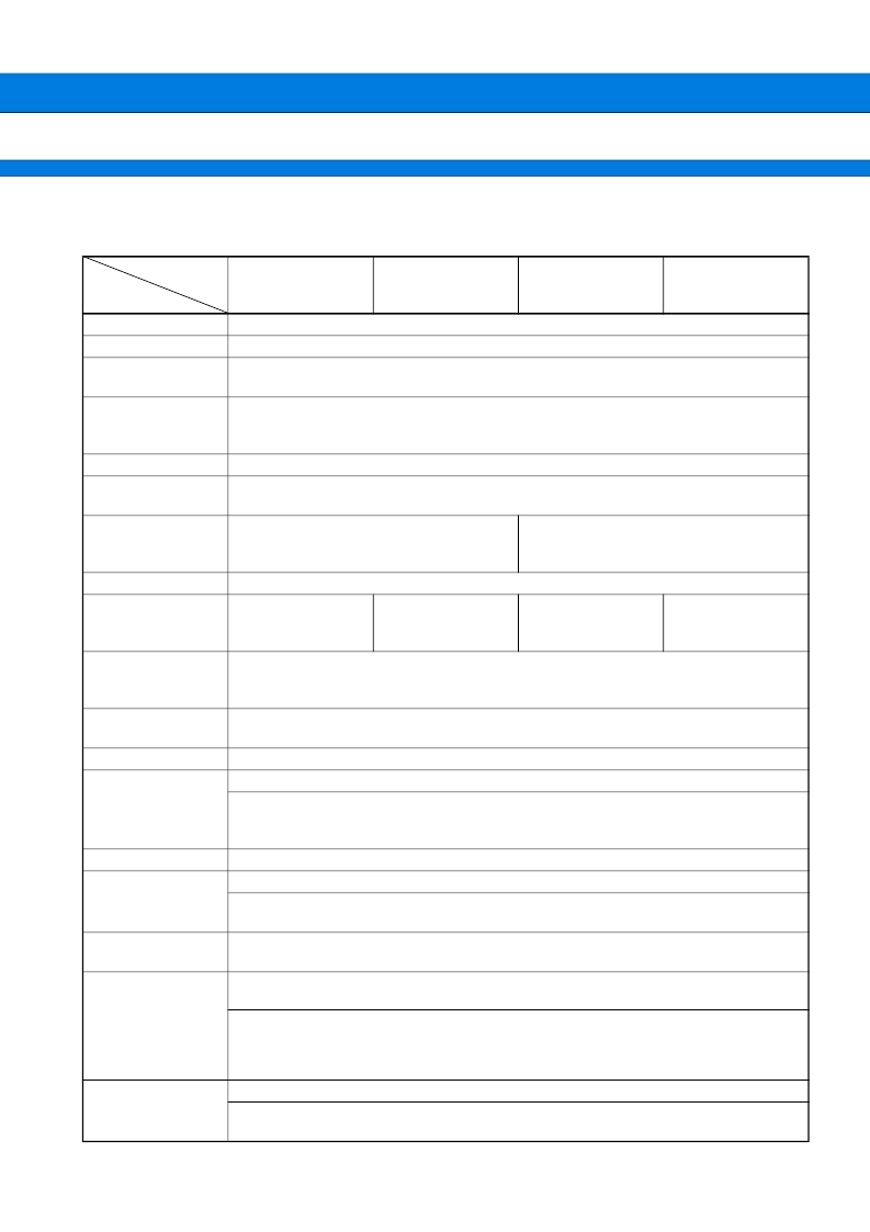
MB90350E Series
5
■
PRODUCT LINEUP1 (Without Clock supervisor function)
Flash memory products
Part Number
MB90F351E,
MB90F352E
(Continued)
Parameter
Type
CPU
MB90F351TE,
MB90F352TE
MB90F351ES,
MB90F352ES
MB90F351TES,
MB90F352TES
Flash memory products
F
2
MC-16LX CPU
System clock
PLL clock multiplication circuit (
×
1,
×
2,
×
3,
×
4,
×
6, 1/2 when PLL stops)
Minimum instruction execution time : 42 ns (oscillation clock 4 MHz, PLL
×
6)
64 Kbytes Flash memory : MB90F351E(S), MB90F351TE(S)
128 Kbytes Dual operation Flash memory (Erase/write and read can be operated at the
same time) : MB90F352E(S), MB90F352TE(S)
4 Kbytes
ROM
RAM
Emulator-specific
power supply*
1
Sub clock pin
(X0A, X1A)
(Max 100 kHz)
Clock supervisor
Low voltage/CPU
operation detection
reset
Yes
No
No
No
Yes
No
Yes
Operating voltage
3.5 V to 5.5 V : at normal operating (not using A/D converter)
4.0 V to 5.5 V : at using A/D converter/Flash programming
4.5 V to 5.5 V : at using external bus
Operating
temperature
Package
40
°
C to
+
125
°
C
LQFP-64
2 channels
UART
Wide range of baud rate settings using a dedicated reload timer
Special synchronous options for adapting to different synchronous serial protocols
LIN functionality working either as master or slave LIN device
1 channel
15 channels
10-bit or 8-bit resolution
Conversion time : Min 3
μ
s includes sample time (per one channel)
Operation clock frequency : fsys/2
1
, fsys/2
3
, fsys/2
5
(fsys
=
Machine clock frequency)
Supports External Event Count function.
I/O Timer 0 (clock input FRCK0) corresponds to ICU0/1.
I/O Timer 1 (clock input FRCK1) corresponds to ICU4/5/6/7, OCU4/5/6/7.
Signals an interrupt when overflowing.
Supports Timer Clear when it matches Output Compare (ch.0, ch.4) .
Operation clock frequency : fsys, fsys/2
1
, fsys/2
2
, fsys/2
3
, fsys/2
4
, fsys/2
5
, fsys/2
6
, fsys/2
7
(fsys
=
Machine clock frequency)
4 channels
Signals an interrupt when 16-bit I/O Timer matches with output compare registers.
A pair of compare registers can be used to generate an output signal.
I
2
C (400 kbps)
A/D converter
16-bit reload timer
(2 channels)
16-bit I/O timer
(2 channels)
16-bit output
compare
相關(guān)PDF資料 |
PDF描述 |
|---|---|
| MB90F356TEPMC1 | 16-bit Proprietary Microcontrollers |
| MB90F356TESPMC | 16-bit Proprietary Microcontrollers |
| MB90F356TESPMC1 | 16-bit Proprietary Microcontrollers |
| MB90F357E | 16-bit Proprietary Microcontrollers |
| MB90F351EPMC | 16-bit Proprietary Microcontrollers |
相關(guān)代理商/技術(shù)參數(shù) |
參數(shù)描述 |
|---|---|
| MB90F362ESPMCR-GE1 | 制造商:FUJITSU 功能描述: |
| MB90F362ESPMCR-G-JNE1 | 制造商:FUJITSU 功能描述: |
| MB90F362TESPMCRGE1 | 制造商:FUJI 功能描述:Pb Free |
| MB90F362TESPMCR-GE1 | 制造商:FUJITSU 功能描述:MCU 16BIT 16LX 64K FLASH 48LQFP 制造商:FUJITSU 功能描述:MCU, 16BIT, 16LX, 64K FLASH, 48LQFP, Controller Family/Series:F2MC-16LX, Core Si |
| MB90F362TESPMCR-G-JNE1 | 制造商:FUJITSU 功能描述: |
發(fā)布緊急采購(gòu),3分鐘左右您將得到回復(fù)。