- 您現(xiàn)在的位置:買賣IC網(wǎng) > PDF目錄377924 > MB90F356E (Fujitsu Limited) 16-bit Proprietary Microcontrollers PDF資料下載
參數(shù)資料
| 型號: | MB90F356E |
| 廠商: | Fujitsu Limited |
| 英文描述: | 16-bit Proprietary Microcontrollers |
| 中文描述: | 16位微控制器專有 |
| 文件頁數(shù): | 17/85頁 |
| 文件大小: | 880K |
| 代理商: | MB90F356E |
第1頁第2頁第3頁第4頁第5頁第6頁第7頁第8頁第9頁第10頁第11頁第12頁第13頁第14頁第15頁第16頁當(dāng)前第17頁第18頁第19頁第20頁第21頁第22頁第23頁第24頁第25頁第26頁第27頁第28頁第29頁第30頁第31頁第32頁第33頁第34頁第35頁第36頁第37頁第38頁第39頁第40頁第41頁第42頁第43頁第44頁第45頁第46頁第47頁第48頁第49頁第50頁第51頁第52頁第53頁第54頁第55頁第56頁第57頁第58頁第59頁第60頁第61頁第62頁第63頁第64頁第65頁第66頁第67頁第68頁第69頁第70頁第71頁第72頁第73頁第74頁第75頁第76頁第77頁第78頁第79頁第80頁第81頁第82頁第83頁第84頁第85頁
MB90350E Series
17
(Continued)
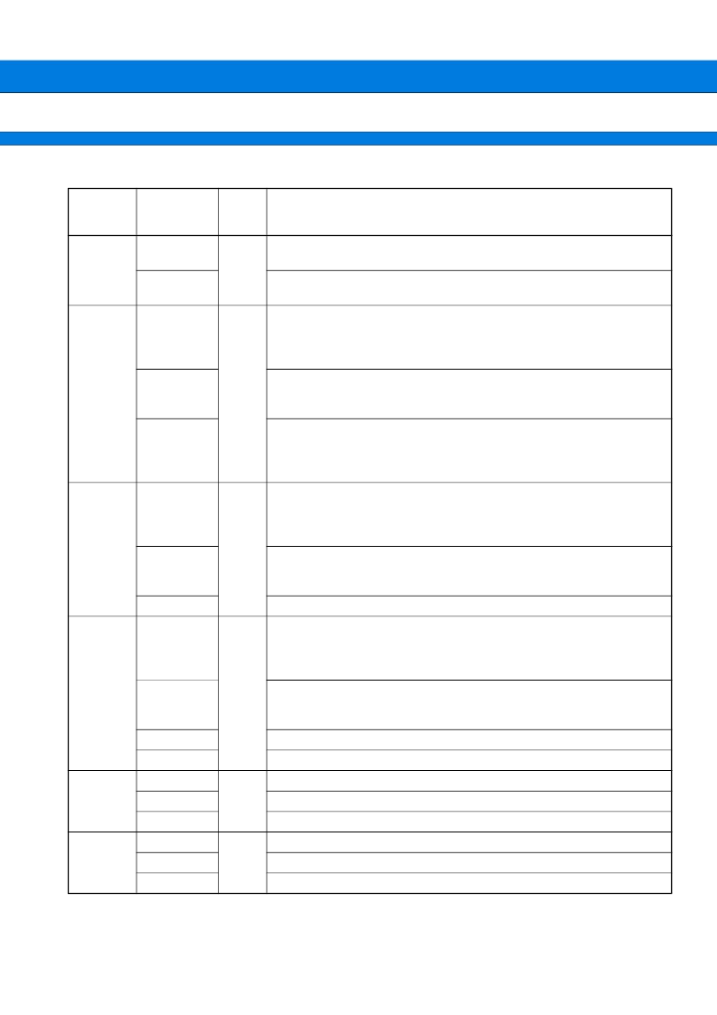
Pin No.
Pin name
I/O
Circuit
type*
Function
39
P17
G
General purpose I/O port. The register can be set to select whether to use
a pull-up resistor. This function is enabled in single-chip mode.
AD15
Input/output pin for external bus address data bus bit 15.
This function is enabled when external bus is enabled.
40 to 43
P20 to P23
G
General purpose I/O ports. The register can be set to select whether to use
a pull-up resistor. In external bus mode, the pins are enabled as a general-
purpose I/O port when the corresponding bit in the external address output
control register (HACR) is 1.
A16 to A19
Output pins for A16 to A19 of the external address data bus.
When the corresponding bit in the external address output control register
(HACR) is 0, the pins are enabled as high address output pins A16 to A19.
PPG9 (8) ,
PPGB (A) ,
PPGD (C) ,
PPGF (E)
Output pins for PPGs
44
P24
G
General purpose I/O port. The register can be set to select whether to use
a pull-up resistor. In external bus mode, the pin is enabled as a general-
purpose I/O port when the corresponding bit in the external address output
control register (HACR) is 1.
A20
Output pin for A20 of the external address data bus. When the correspond-
ing bit in the external address output control register (HACR) is 0, the pin is
enabled as high address output pin A20.
IN0
Data sample input pin for input capture ICU0
51
P25
G
General purpose I/O port. The register can be set to select whether to use
a pull-up resistor. In external bus mode, the pin is enabled as a general-
purpose I/O port when the corresponding bit in the external address output
control register (HACR) is 1.
A21
Output pin for A21 of the external address data bus. When the correspond-
ing bit in the external address output control register (HACR) is 0, the pin is
enabled as high address output pin A21.
IN1
Data sample input pin for input capture ICU1
ADTG
Trigger input pin for A/D converter
52
P44
H
General purpose I/O port
SDA0
Serial data I/O pin for I
2
C 0
FRCK0
Input pin for the 16-bit I/O Timer 0
53
P45
H
General purpose I/O port
SCL0
Serial clock I/O pin for I
2
C 0
FRCK1
Input pin for the 16-bit I/O Timer 1
相關(guān)PDF資料 |
PDF描述 |
|---|---|
| MB90F356EPMC | 16-bit Proprietary Microcontrollers |
| MB90F356EPMC1 | 16-bit Proprietary Microcontrollers |
| MB90F356ESPMC | 16-bit Proprietary Microcontrollers |
| MB90F356ESPMC1 | 16-bit Proprietary Microcontrollers |
| MB90F356TE | 16-bit Proprietary Microcontrollers |
相關(guān)代理商/技術(shù)參數(shù) |
參數(shù)描述 |
|---|---|
| MB90F362ESPMCR-GE1 | 制造商:FUJITSU 功能描述: |
| MB90F362ESPMCR-G-JNE1 | 制造商:FUJITSU 功能描述: |
| MB90F362TESPMCRGE1 | 制造商:FUJI 功能描述:Pb Free |
| MB90F362TESPMCR-GE1 | 制造商:FUJITSU 功能描述:MCU 16BIT 16LX 64K FLASH 48LQFP 制造商:FUJITSU 功能描述:MCU, 16BIT, 16LX, 64K FLASH, 48LQFP, Controller Family/Series:F2MC-16LX, Core Si |
| MB90F362TESPMCR-G-JNE1 | 制造商:FUJITSU 功能描述: |
發(fā)布緊急采購,3分鐘左右您將得到回復(fù)。