- 您現(xiàn)在的位置:買賣IC網(wǎng) > PDF目錄69021 > MB90947APF MICROCONTROLLER, PQFP100 PDF資料下載
參數(shù)資料
| 型號: | MB90947APF |
| 元件分類: | 微控制器/微處理器 |
| 英文描述: | MICROCONTROLLER, PQFP100 |
| 封裝: | 14 X 20 MM, 3.35 MM HEIGHT, 0.65 MM PITCH, PLASTIC, QFP-100 |
| 文件頁數(shù): | 18/57頁 |
| 文件大小: | 1586K |
| 代理商: | MB90947APF |
第1頁第2頁第3頁第4頁第5頁第6頁第7頁第8頁第9頁第10頁第11頁第12頁第13頁第14頁第15頁第16頁第17頁當(dāng)前第18頁第19頁第20頁第21頁第22頁第23頁第24頁第25頁第26頁第27頁第28頁第29頁第30頁第31頁第32頁第33頁第34頁第35頁第36頁第37頁第38頁第39頁第40頁第41頁第42頁第43頁第44頁第45頁第46頁第47頁第48頁第49頁第50頁第51頁第52頁第53頁第54頁第55頁第56頁第57頁
SINGLE-CHIP 8-BIT CMOS MICROCOMPUTER
7544 Group
MITSUBISHI MICROCOMPUTERS
25
PRELIMINAR
Y
Notice:
This
is not
a final
specification.
Som
e parametric
limits
are
subject
to change.
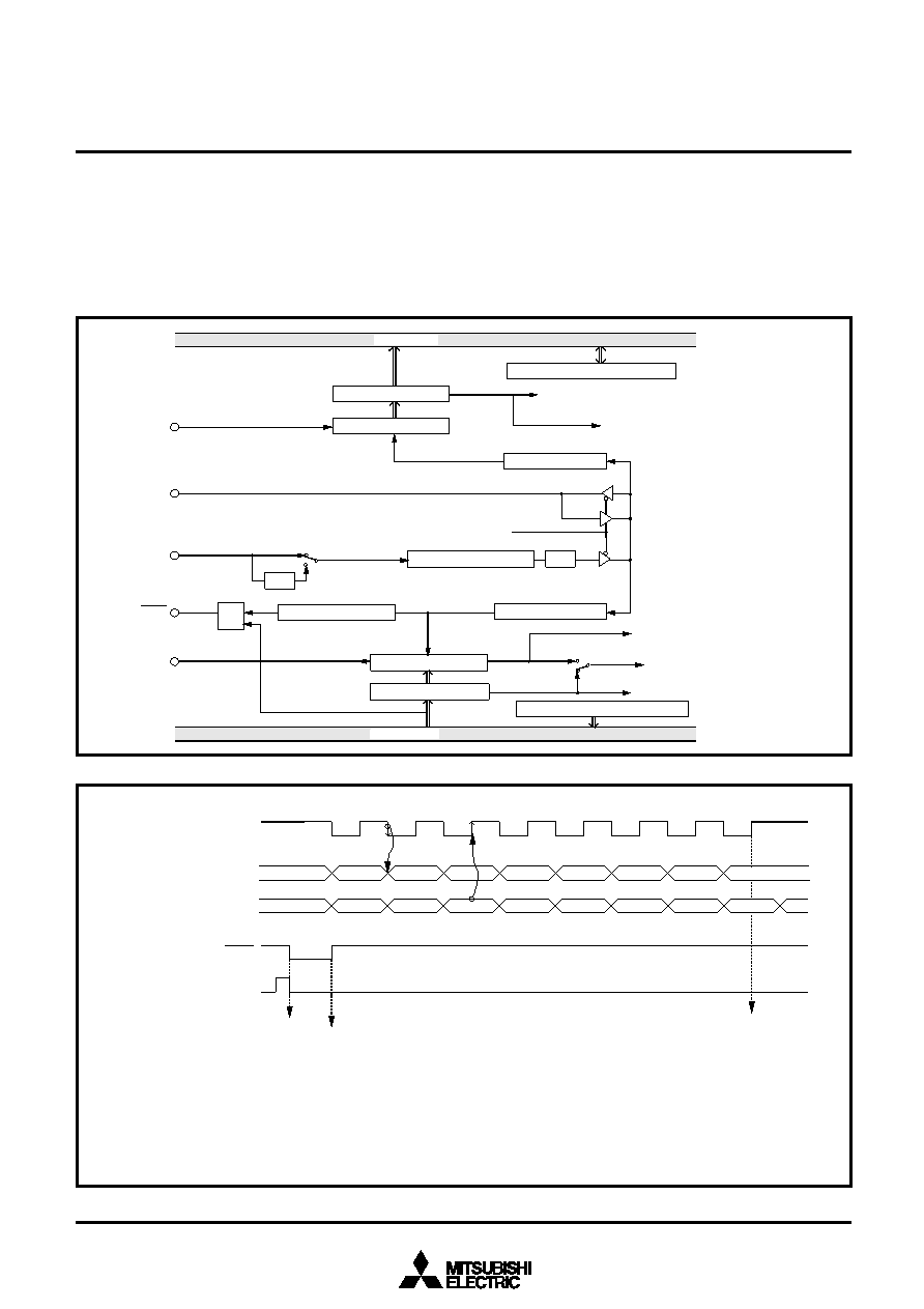
Fig. 26 Block diagram of clock synchronous serial I/O
Fig. 27 Operation of clock synchronous serial I/O function
Serial I/O
qSerial I/O
Serial I/O can be used as either clock synchronous or asynchro-
nous (UART) serial I/O. A dedicated timer is also provided for
baud rate generation.
(1) Clock Synchronous Serial I/O Mode
Clock synchronous serial I/O mode can be selected by setting the
serial I/O mode selection bit of the serial I/O control register (bit 6)
to “1”.
For clock synchronous serial I/O, the transmitter and the receiver
must use the same clock. If an internal clock is used, transfer is
started by a write signal to the TB/RB.
1/4
F/F
P12/SCLK
Serial I/O status register
Serial I/O control register
P13/SRDY
P10/RXD
P11/TXD
XIN
Receive buffer register
Address 001816
Receive shift register
Receive buffer full flag (RBF)
Receive interrupt request (RI)
Clock control circuit
Shift clock
Serial I/O synchronous
clock selection bit
Frequency division ratio 1/(n+1)
Baud rate generator
Address 001C16
BRG count source selection bit
Clock control circuit
Falling-edge detector
Transmit buffer register
Data bus
Address 001816
Shift clock
Transmit shift completion flag (TSC)
Transmit buffer empty flag (TBE)
Transmit interrupt request (TI)
Transmit interrupt source selection bit
Address 001916
Data bus
Address 001A16
Transmit shift register
D7
D0
D1
D2
D3
D4
D5
D6
D0
D1
D2
D3
D4
D5
D6
RBF = 1
TSC = 1
TBE = 0
TBE = 1
TSC = 0
Transfer shift clock
(1/2 to 1/2048 of the internal
clock, or an external clock)
Serial output TxD
Serial input RxD
Write pulse to receive/transmit
buffer register (address 001816)
Overrun error (OE)
detection
Notes 1: As the transmit interrupt (TI), which can be selected, either when the transmit buffer has emptied (TBE=1) or after
the transmit shift operation has ended (TSC=1), by setting the transmit interrupt source selection bit (TIC) of the
serial I/O1 control register.
2: If data is written to the transmit buffer register when TSC=0, the transmit clock is generated continuously and serial
data is output continuously from the TxD pin.
3: The receive interrupt (RI) is set when the receive buffer full flag (RBF) becomes “1” .
Receive enable signal SRDY
相關(guān)PDF資料 |
PDF描述 |
|---|---|
| MB90F947PF | 16-BIT, FLASH, 24 MHz, MICROCONTROLLER, PQFP100 |
| MB90F949PF | 16-BIT, FLASH, 24 MHz, MICROCONTROLLER, PQFP100 |
| MB90F967SPMT | 16-BIT, FLASH, 24 MHz, MICROCONTROLLER, PQFP48 |
| MB90P214PF | 16-BIT, OTPROM, 16 MHz, MICROCONTROLLER, PQFP80 |
| MB90W214BZF | 16-BIT, UVPROM, 16 MHz, MICROCONTROLLER, CQFP80 |
相關(guān)代理商/技術(shù)參數(shù) |
參數(shù)描述 |
|---|---|
| MB90F334APMC1-GE1 | 制造商:FUJITSU 功能描述: |
| MB90F334APMC1-G-SPE1 | 制造商:FUJITSU 功能描述: |
| MB90F334APMC-G-JNE1 | 制造商:FUJITSU 功能描述: |
| MB90F334APMC-G-SNE1 | 制造商:FUJITSU 功能描述: |
| MB90F334APMC-G-SPE1 | 制造商:FUJITSU 功能描述: |
發(fā)布緊急采購,3分鐘左右您將得到回復(fù)。