- 您現(xiàn)在的位置:買賣IC網(wǎng) > PDF目錄377895 > MB88111 (Fujitsu Limited) Analog-to-Digital Converter(二十四通道串行接口A/D轉(zhuǎn)換器) PDF資料下載
參數(shù)資料
| 型號(hào): | MB88111 |
| 廠商: | Fujitsu Limited |
| 英文描述: | Analog-to-Digital Converter(二十四通道串行接口A/D轉(zhuǎn)換器) |
| 中文描述: | 模擬到數(shù)字轉(zhuǎn)換器(二十四通道串行接口的A / D轉(zhuǎn)換器) |
| 文件頁(yè)數(shù): | 4/26頁(yè) |
| 文件大小: | 243K |
| 代理商: | MB88111 |
第1頁(yè)第2頁(yè)第3頁(yè)當(dāng)前第4頁(yè)第5頁(yè)第6頁(yè)第7頁(yè)第8頁(yè)第9頁(yè)第10頁(yè)第11頁(yè)第12頁(yè)第13頁(yè)第14頁(yè)第15頁(yè)第16頁(yè)第17頁(yè)第18頁(yè)第19頁(yè)第20頁(yè)第21頁(yè)第22頁(yè)第23頁(yè)第24頁(yè)第25頁(yè)第26頁(yè)
4
MB88111
I
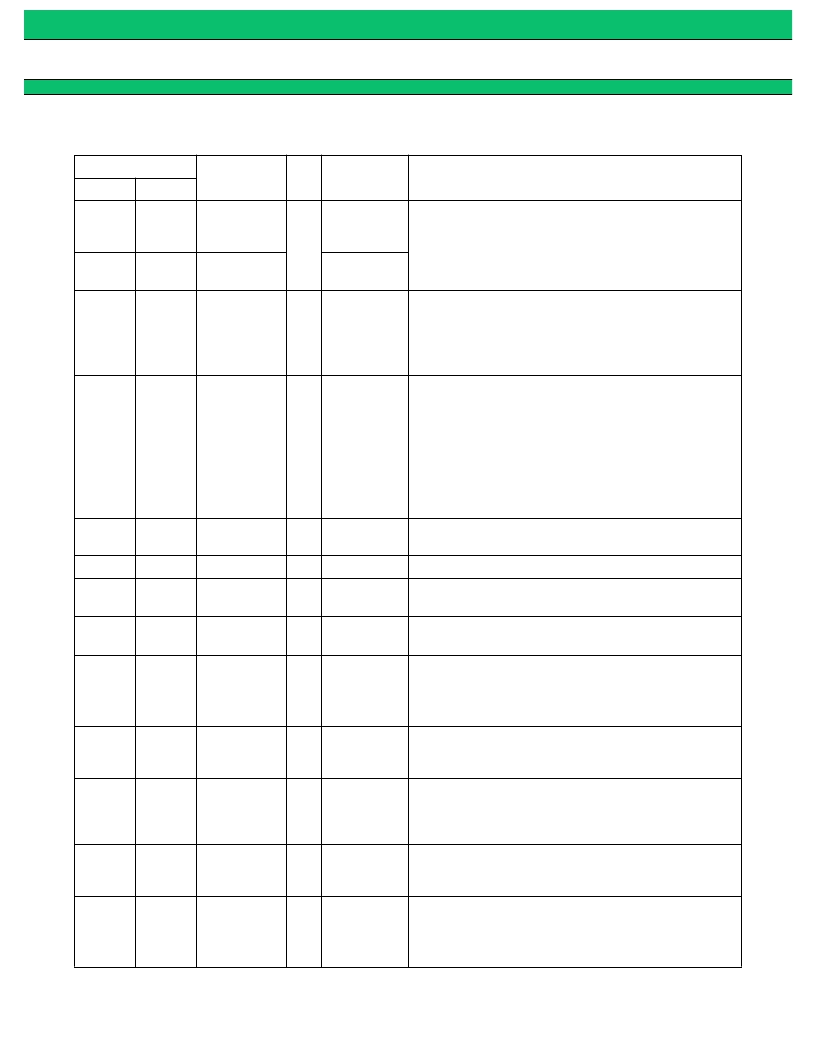
PIN DESCRIPTION
(Continued)
Pin no.
Symbol
I/O
Circuit type
Descriptions
QFP
DIP
41 to 26
2 to 1,
48 to 43,
41 to 34
AN0 to AN15
I
F
Analog input pins. The pin to be subject to conversion
is selected by the command input through the SIN pin.
Also, a series of pins from AN16 to AN23 can be used
as a port input.
25 to 18 33 to 31,
29 to 25
AN16 to
AN23
G
12
19
MOD
I
A
Pin for selecting a serial data output mode:
“L”: Mode A for output from the SOT pin in
synchronization with the fall of the SCK signal.
“H”: Mode B for output from the SOT pin in
synchronization with the rise of the SCK signal.
11
10
17
16
CS1
CS2X
I
A
Input pins for selecting an extended serial interface
mode.
Setting the CS1 level to “H” and the CS2X level to “L”
enables A/D converted data transfer. Setting the CS1
level to “L” or the CS2X level to “H” clears the register
command without affecting A/D conversion. Serial
data input to the external extended serial input pin
ESIN is output to the SOT pin as it is. (See Section 7
“Extended Serial Interface” in “
I
OPERATION.”)
4
10
SIN
I
B
Serial data input pin
This pin is a hysteresis input with a filter.
6
12
SOT
O
H
Serial data output pin
3
9
CCLK
I
B
System clock input pin
This pin is a hysteresis input.
2
8
SCK
I
B
Serial data transfer clock input pin
This pin is a hysteresis input with a filter.
9
15
ATGX
I
C
External trigger input pin. This pin incorporates a pull-
up resistor. The ATC command initiates A/D conversion
at the rise of the signal at this pin.
The pin is a hysteresis input.
8
14
IRQX
O
H
A/D conversion interrupt signal input pin. The signal
level becomes “L” upon completion of A/D conversion;
it becomes “H” upon reception of data to be converted.
7
13
ENDC
O
H
A/D conversion completion signal output pin. The
signal level becomes “H” upon completion of A/D
conversion; it becomes “L” upon reception of data to be
converted.
5
11
ESIN
I
A
Serial input extension input pin. When the CS1 level is
“L” or the CS2X level is “H,” data input to the ESIN pin
is output to the SOT pin as it is.
1
7
RSTX
I
D
Reset signal input pin. This pin incorporates a pull-up
resistor. Setting the signal level to “L” initializes the
internal circuit of the device.
This pin is a hysteresis input with a filter.
相關(guān)PDF資料 |
PDF描述 |
|---|---|
| MB88141A | D/A Converter for Digital Tuning (Compatible with I2C Bus) |
| MB88141AP | ER 35C 35#16 PIN RECP WALL |
| MB88141APF | D/A Converter for Digital Tuning (Compatible with I2C Bus) |
| MB88141APFV | D/A Converter for Digital Tuning (Compatible with I2C Bus) |
| MB88141PF | D/A Converter for Digital Tuning (With Built-in OP Amp and I/O Expander) |
相關(guān)代理商/技術(shù)參數(shù) |
參數(shù)描述 |
|---|---|
| MB88111PFQ | 制造商:FUJITSU 制造商全稱:Fujitsu Component Limited. 功能描述:A/D Converter (With 24-Channel Input at 10-bit Resolution) |
| MB88111P-SH | 制造商:FUJITSU 制造商全稱:Fujitsu Component Limited. 功能描述:A/D Converter (With 24-Channel Input at 10-bit Resolution) |
| MB88121BPFV-ESE2 | 制造商:FUJITSU 功能描述: |
| MB88121BPFV-GSE1 | 制造商:FUJITSU 功能描述: |
| MB88121C | 制造商:FUJITSU 制造商全稱:Fujitsu Component Limited. 功能描述:The Ultimate Automotive Network |
發(fā)布緊急采購(gòu),3分鐘左右您將得到回復(fù)。