- 您現(xiàn)在的位置:買賣IC網(wǎng) > PDF目錄377894 > MB86832-66PFV (FUJITSU LTD) 32-bit Embedded Controller PDF資料下載
參數(shù)資料
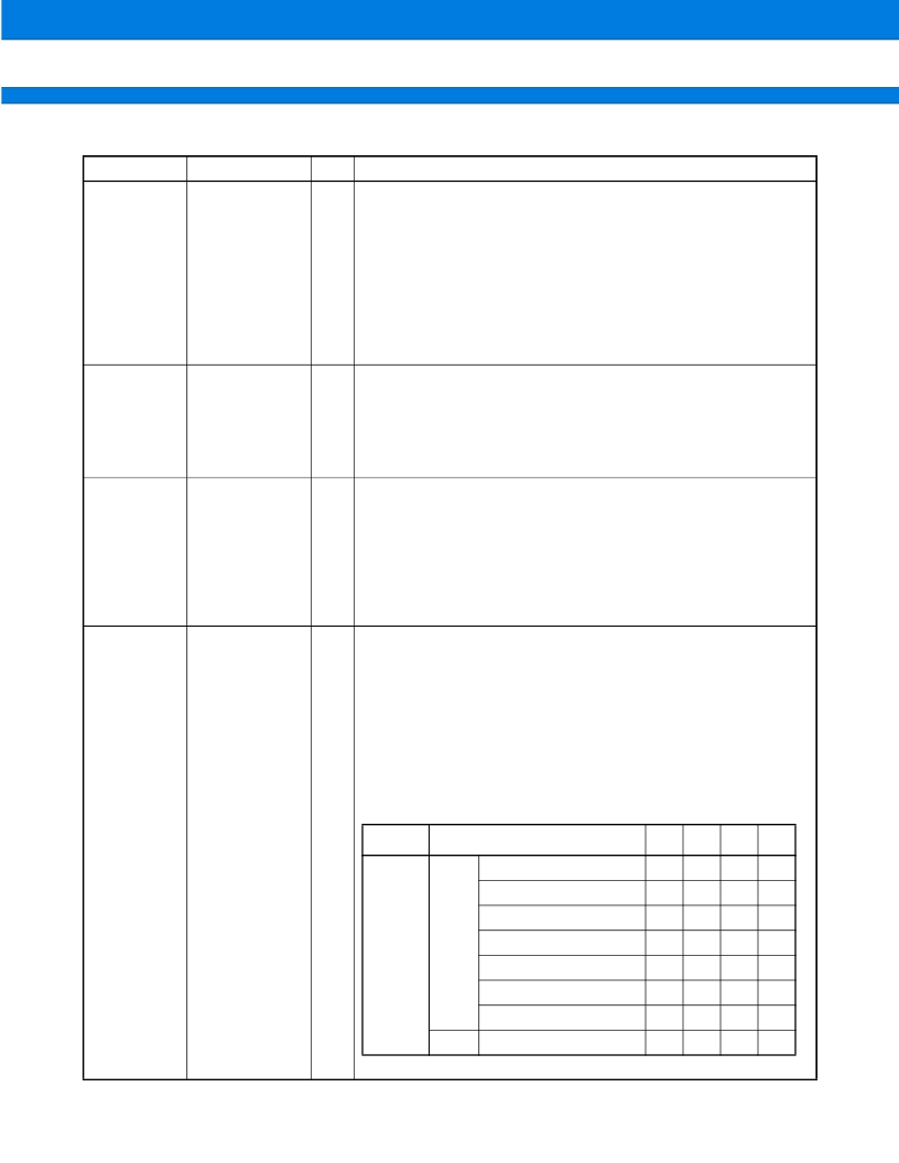
| 型號: | MB86832-66PFV |
| 廠商: | FUJITSU LTD |
| 元件分類: | 微控制器/微處理器 |
| 英文描述: | 32-bit Embedded Controller |
| 中文描述: | 32-BIT, 66 MHz, RISC MICROCONTROLLER, PQFP176 |
| 封裝: | 24 X 24 MM, PLASTIC, QFP-176 |
| 文件頁數(shù): | 11/82頁 |
| 文件大小: | 1373K |
| 代理商: | MB86832-66PFV |
第1頁第2頁第3頁第4頁第5頁第6頁第7頁第8頁第9頁第10頁當前第11頁第12頁第13頁第14頁第15頁第16頁第17頁第18頁第19頁第20頁第21頁第22頁第23頁第24頁第25頁第26頁第27頁第28頁第29頁第30頁第31頁第32頁第33頁第34頁第35頁第36頁第37頁第38頁第39頁第40頁第41頁第42頁第43頁第44頁第45頁第46頁第47頁第48頁第49頁第50頁第51頁第52頁第53頁第54頁第55頁第56頁第57頁第58頁第59頁第60頁第61頁第62頁第63頁第64頁第65頁第66頁第67頁第68頁第69頁第70頁第71頁第72頁第73頁第74頁第75頁第76頁第77頁第78頁第79頁第80頁第81頁第82頁
MB86830 Series
11
(Continued)
Symbol
(Continued)
Pin name
I/O
Function
D<31:0>
DATA BUS
I/O
Data bus signal.
This pin provides a bidirectional data bus used for instruction fetch,
data load, and data store operations. Instructions and word data must
be aligned at addresses which are multiples of the number 4.
Half words and double words must be aligned at addresses which are
multiples of the numbers 2 and 8, respectively. D<7:0> and D<15:0>
are used in the 8-bit and 16-bit bus modes, respectively. For use in the
16-bit bus mode, a pull-up resistor must be connected to the data bus
which is not used (D<31:8> for the 8-bit bus and D<31:16> for the 16-
bit bus).
AS#
ADDRESS
STROBE
I/O
Address strobe signal.
This pin outputs the “L” level signal for the first bus cycle. Basically, the
bus cycle starts with the AS# signal asserted and ends up with the
READY# or RDYOUT# signal asserted.
In the bus grant state, the pin serves as an input used for the signals to
actuate the CS generator and wait state generator circuits.
RDWR#
READ/WRITE
BUS
TRANSACTION
I/O
Read/write signal.
This pin outputs the “L” level signal when the current bus cycle is the
write cycle or the “H” level signal when it is the read or idle cycle. The
output level remains at “H” or“L” during the entire bus cycle from the be-
ginning to end.
In the bus grant state, the pin serves as an input used for generating
the DWE0#-DWE3# and DOE# signals to enable the DRAM controller.
The signal at this pin is not used when the DRAM controller is disabled.
BE0#
BE1#
BE2#
BE3#
BYTE ENABLE
O
O
I/O
O
Bye enable signals.
These pins are used to indicate the bytes valid for in write mode when
the 32-bit bus width is used.
In read mode, all of the BE0# to BE3# signals are asserted regardless
of the data type. For the 8-bit or 16-bit bus width, the BE2# and BE3#
pins output ADR<1> and ADR<0>, respectively.
The BE0# to BE3# pins remain enabled during the bus cycle; the out-
put level during the idle cycle is not guaranteed.
In the bus grant state, the pins enter the High-Z state and, only when
the DRAM controller is on with the 16-bit bus width used, the BE2# pin
serves as the ADR<1> input pin.
(Continued)
Width of
bus
Access type
BE0#
BE1#
BE2#
BE3#
Width of
32-bits
bus
Write
Byte-0 (D<31:24>) *
0
1
1
1
Byte-1 (D<23:16>)
1
0
1
1
Byte-2 (D<15:8>)
1
1
0
1
Byte-3 (D<7:0>)
1
1
1
0
Half word-0(D<31:16>)
0
0
1
1
Half word-1(D<15:0>)
1
1
0
0
Word
0
0
0
0
Read
All data types
0
0
0
0
相關(guān)PDF資料 |
PDF描述 |
|---|---|
| MB86833 | 32-bit Embedded Controller |
| MB86833PMT2 | 32-bit Embedded Controller |
| MB86834 | 32-bit Embedded Controller |
| MB86834-120PFV | 32-bit Embedded Controller |
| MB86834PFV | 32-bit Embedded Controller |
相關(guān)代理商/技術(shù)參數(shù) |
參數(shù)描述 |
|---|---|
| MB86832-80PFV | 制造商:FUJITSU 制造商全稱:Fujitsu Component Limited. 功能描述:32-bit Embedded Controller |
| MB86833 | 制造商:FUJITSU 制造商全稱:Fujitsu Component Limited. 功能描述:32-bit Embedded Controller |
| MB86833PMT2 | 制造商:FUJITSU 制造商全稱:Fujitsu Component Limited. 功能描述:32-bit Embedded Controller |
| MB86834 | 制造商:FUJITSU 制造商全稱:Fujitsu Component Limited. 功能描述:32-bit Embedded Controller |
| MB86834-120PFV | 制造商:FUJITSU 制造商全稱:Fujitsu Component Limited. 功能描述:32-bit Embedded Controller |
發(fā)布緊急采購,3分鐘左右您將得到回復(fù)。