- 您現(xiàn)在的位置:買賣IC網(wǎng) > PDF目錄377894 > MB86612 (Fujitsu Limited) IEEE 1394 Bus Controller (for MPEG, DVC) PDF資料下載
參數(shù)資料
| 型號: | MB86612 |
| 廠商: | Fujitsu Limited |
| 英文描述: | IEEE 1394 Bus Controller (for MPEG, DVC) |
| 中文描述: | 1394總線控制器(用于MPEG,抵境證明書) |
| 文件頁數(shù): | 9/40頁 |
| 文件大?。?/td> | 574K |
| 代理商: | MB86612 |
第1頁第2頁第3頁第4頁第5頁第6頁第7頁第8頁當(dāng)前第9頁第10頁第11頁第12頁第13頁第14頁第15頁第16頁第17頁第18頁第19頁第20頁第21頁第22頁第23頁第24頁第25頁第26頁第27頁第28頁第29頁第30頁第31頁第32頁第33頁第34頁第35頁第36頁第37頁第38頁第39頁第40頁
9
MB86612
I
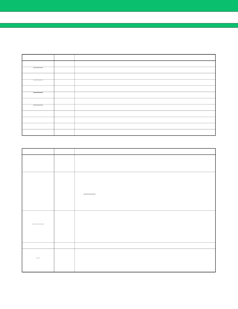
PIN DESCRIPTION
1. 1394 Interface
2. Isochronous-data Interface
(Continued)
Pin name
TPA0
TPA0
TPB0
TPB0
TPA1
TPA1
TPB1
TPB1
TPBIAS0
TPBIAS1
RO0
RO1
I/O
I/O
I/O
I/O
I/O
I/O
I/O
I/O
I/O
O
O
O
O
Function
Cable port 0 TPA positive signal I/O pin
Cable port 0 TPA negative signal I/O pin
Cable port 0 TPB positive signal I/O pin
Cable port 0 TPB negative signal I/O pin
Cable port 1 TPA positive signal I/O pin
Cable port 1 TPA negative signal I/O pin
Cable port 1 TPB positive signal I/O pin
Cable port 1 TPB negative signal I/O pin
Cable port 0 common voltage reference voltage output pin
Cable port 1 common voltage reference voltage output pin
Connect to GND through 4.7 k
resistance
Connect to GND through 4.7 k
resistance
Pin name
I/O
Function
ICLK
I
Isochronous data interface CLK signal input pin (DC to 16 MHz).
Note: When this clock is stopped, transfer is stopped. Also the “Data FIFO init
(63h)” instruction (operand: 21) is invalid.
Isochronous transfer sending/receiving switching signal input pin.
0 input: Clear ISO FIFO, go to sending mode.
Sending starts after receiving 1 packet of data.
1 input: Clear ISO FIFO, go to receiving mode. If a ‘1’ signal is entered during
packet sending, receiving mode begins after sending of the current packet.
The ILWRE signal is asserted after receiving 1 packet.
IDIR
I
Note: This signal should normally be left at ‘1’, and switched to ‘0’ only when
sending.
Isochronous FIFE access enable signal output pin.
Sending: Asserted when 1 or more empty source packets are present in ISO
FIFO.
When negated, the data output up to the leading edge for the next ICLX.
Receiving: Asserted when receiving of 1 source packet of data is completed.
Negate conditions for this signal are determined by the ilwre-mode bit (bit 11) in
the mode-control register.
Isochronous transfer data input/output bits. (MSB is ID7, LSB is ID0)
ID7 to ID0 enable signal input pin.
Sending: While this signal is active, data from the ID7 to ID0 pins is loaded into
ISO FIFO memory at the rising edge of the ICLK signal.
Receiving: While this signal is active, data from ISO FIFO memory is sent to the
ID7 to ID0 pins. Data is switched at the falling edge of the ICLK signal.
ILWRE
O
ID7 to ID0
I/O
IV
I
相關(guān)PDF資料 |
PDF描述 |
|---|---|
| MB86612PBT | IEEE 1394 Bus Controller (for MPEG, DVC) |
| MB86612PFV | IEEE 1394 Bus Controller (for MPEG, DVC) |
| MB86613 | RES 3.0 OHM 1/16W 5% 0402 SMD |
| MB86613PBT | IEEE 1394 Open HCI Controller |
| MB86613PFV | IEEE 1394 Open HCI Controller |
相關(guān)代理商/技術(shù)參數(shù) |
參數(shù)描述 |
|---|---|
| MB86612PBT | 制造商:FUJITSU 制造商全稱:Fujitsu Component Limited. 功能描述:IEEE 1394 Bus Controller (for MPEG, DVC) |
| MB86612PFV | 制造商:FUJITSU 制造商全稱:Fujitsu Component Limited. 功能描述:IEEE 1394 Bus Controller (for MPEG, DVC) |
| MB86613 | 制造商:FUJITSU 制造商全稱:Fujitsu Component Limited. 功能描述:IEEE 1394 Open HCI Controller |
| MB86613PBT | 制造商:FUJITSU 制造商全稱:Fujitsu Component Limited. 功能描述:IEEE 1394 Open HCI Controller |
| MB86613PFV | 制造商:FUJITSU 制造商全稱:Fujitsu Component Limited. 功能描述:IEEE 1394 Open HCI Controller |
發(fā)布緊急采購,3分鐘左右您將得到回復(fù)。