- 您現(xiàn)在的位置:買賣IC網(wǎng) > PDF目錄5538 > MAX9923FEUB+ (Maxim Integrated Products)IC AMP CURRENT SENSE 10-MSOP PDF資料下載
參數(shù)資料

MAX9922/MAX9923
Ultra-Precision, High-Side
Current-Sense Amplifiers
_______________________________________________________________________________________
5
Note 1:
All devices are 100% production tested at TA = +85°C. All temperature limits are guaranteed by design.
Note 2:
VOS is measured in bidirectional mode with VREF = VDD/2.
Note 3:
Data sheet limits are guaranteed by design and bench characterization. Thermocouple effects preclude measurement of
this parameter during production testing. Devices are screened during production testing to eliminate defective units.
Note 4:
VOS drift limits are guaranteed by design and bench characterization and are the average of drift from -40°C to +25°C and
from +25°C to +85°C.
Note 5:
VRSB = VRS+ = 12V, VREF = VDD/2 for bipolar mode and VREF = 0V for unipolar mode. Gain accuracy and gain linearity are
specified over a VSENSE range that keeps the output voltage 250mV away from the rails to achieve full accuracy. Output of
the part is rail-to-rail, and goes to within 25mV of the rails, but accuracy is not maintained. Linear operation is not guaran-
teed for VSENSE voltages > ±150mV. See the Typical Operating Characteristics section for plots of Input vs. Output.
Note 6:
This is the worst-case REF current needed to directly drive the bottom terminal of the gain setting resistors, at VDD = 3.3V,
and VREF = VDD/2 while maintaining gain accuracy. An internal 1k resistor (R1) is present in the MAX9923T/
MAX9923H/MAX9923F between the FB and REF pins, while in the MAX9922 the resistor is external and user selectable. A
voltage identical to the VSENSE develops across this resistor. In all versions the REF input current is dependent on the mag-
nitude and polarity of VSENSE, and in the MAX9922 it is dependent on the value of the external resistor as well. The input
bias current for REF is typically 1pA in the MAX9922 since it connects to the gate of a MOS transistor. See the
External
Reference section for more details.
Note 7:
The range of VREF, VCM, and VSENSE may limit the output swing of the MAX9922 with adjustable gain set to less than
100V/V.
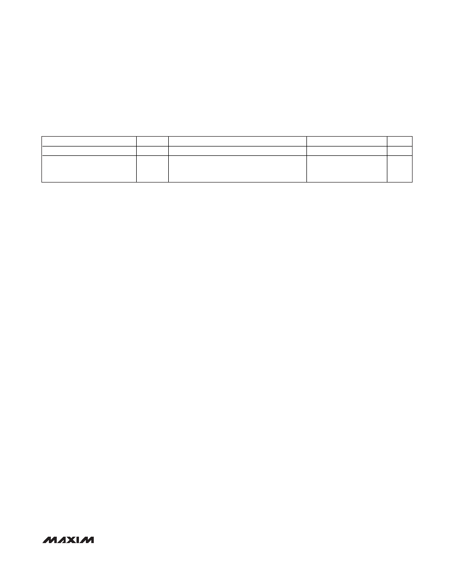
ELECTRICAL CHARACTERISTICS (continued)
(VRSB = VRS+ = VRS- = +12V, VDD = +3.3V, VGND = 0V, VREF = VDD/2 for bidirectional, VREF = 0V for unidirectional, VSENSE = VRS+ - VRS-
= 0V, MAX9922 is set for AV =100V/V (R1 = 1k, R2 = 99k), SHDN = VDD, TA = -40°C to +85°C, unless otherwise noted. Typical values
are at TA = +25°C.) (Note 1)
PARAMETER
SYMBOL
CONDITIONS
MIN
TYP
MAX
UNITS
Power-Down Supply Current
IRSBL
VDD = VREF = 0V, VRSB = VRS+ = VRS- = 28V
0.05
1
A
Power-Up Time
MAX9922, AV = 100V/V, VREF = 0V, VSENSE =
10mV, VDD = 0V to 3.3V, settling to 0.1% of final
value
800
s
相關(guān)PDF資料 |
PDF描述 |
|---|---|
| RCWL0805R620JNEA | RES .62 OHM 1/8W 5% 0805 SMD |
| 1.5KE82HE3/54 | TVS UNIDIR 1.5KW 82V 10% 1.5KE |
| RCWL0805R560JNEA | RES .56 OHM 1/8W 5% 0805 SMD |
| 1.5KE8.2-E3/54 | TVS UNIDIR 1.5KW 8.2V 10% 1.5KE |
| MAX9923HEUB+ | IC AMP CURRENT SENSE 10-MSOP |
相關(guān)代理商/技術(shù)參數(shù) |
參數(shù)描述 |
|---|---|
| MAX9923FEUB+ | 功能描述:電流靈敏放大器 Current-Sense Amplifier RoHS:否 制造商:Texas Instruments 通道數(shù)量: 共模抑制比(最小值):110 dB 輸入補償電壓:80 uV 電源電壓-最大:5.5 V 電源電壓-最小:2.7 V 電源電流:350 uA 最大工作溫度:+ 125 C 最小工作溫度:- 40 C 安裝風(fēng)格:SMD/SMT 封裝 / 箱體:VQFN-16 封裝:Reel |
| MAX9923FEUB+T | 功能描述:電流靈敏放大器 Current-Sense Amplifier RoHS:否 制造商:Texas Instruments 通道數(shù)量: 共模抑制比(最小值):110 dB 輸入補償電壓:80 uV 電源電壓-最大:5.5 V 電源電壓-最小:2.7 V 電源電流:350 uA 最大工作溫度:+ 125 C 最小工作溫度:- 40 C 安裝風(fēng)格:SMD/SMT 封裝 / 箱體:VQFN-16 封裝:Reel |
| MAX9923HABT+T | 制造商:Maxim Integrated Products 功能描述:- Tape and Reel |
| MAX9923HAUB+ | 功能描述:電流靈敏放大器 Current-Sense Amplifier RoHS:否 制造商:Texas Instruments 通道數(shù)量: 共模抑制比(最小值):110 dB 輸入補償電壓:80 uV 電源電壓-最大:5.5 V 電源電壓-最小:2.7 V 電源電流:350 uA 最大工作溫度:+ 125 C 最小工作溫度:- 40 C 安裝風(fēng)格:SMD/SMT 封裝 / 箱體:VQFN-16 封裝:Reel |
| MAX9923HEUB+ | 功能描述:電流靈敏放大器 Current-Sense Amplifier RoHS:否 制造商:Texas Instruments 通道數(shù)量: 共模抑制比(最小值):110 dB 輸入補償電壓:80 uV 電源電壓-最大:5.5 V 電源電壓-最小:2.7 V 電源電流:350 uA 最大工作溫度:+ 125 C 最小工作溫度:- 40 C 安裝風(fēng)格:SMD/SMT 封裝 / 箱體:VQFN-16 封裝:Reel |
發(fā)布緊急采購,3分鐘左右您將得到回復(fù)。