- 您現(xiàn)在的位置:買賣IC網(wǎng) > PDF目錄11684 > MAX9250GCM+T (Maxim Integrated Products)IC DESERIALIZER LVDS 48-LQFP PDF資料下載
參數(shù)資料
| 型號: | MAX9250GCM+T |
| 廠商: | Maxim Integrated Products |
| 文件頁數(shù): | 8/20頁 |
| 文件大?。?/td> | 0K |
| 描述: | IC DESERIALIZER LVDS 48-LQFP |
| 產(chǎn)品培訓(xùn)模塊: | Lead (SnPb) Finish for COTS Obsolescence Mitigation Program |
| 標準包裝: | 2,000 |
| 功能: | 解串器 |
| 數(shù)據(jù)速率: | 840Mbps |
| 輸入類型: | LVDS |
| 輸出類型: | LVCMOS |
| 輸入數(shù): | 1 |
| 輸出數(shù): | 27 |
| 電源電壓: | 3 V ~ 3.6 V |
| 工作溫度: | -40°C ~ 105°C |
| 安裝類型: | 表面貼裝 |
| 封裝/外殼: | 48-LQFP |
| 供應(yīng)商設(shè)備封裝: | 48-LQFP(7x7) |
| 包裝: | 帶卷 (TR) |
MAX9248/MAX9250
27-Bit, 2.5MHz to 42MHz
DC-Balanced LVDS Deserializers
16
______________________________________________________________________________________
Spread-Spectrum Selection
The MAX9248 single-ended data and clock outputs are
programmable for a variation of ±2% or ±4% around
the LVDS input clock frequency. The modulation rate of
the frequency variation is 32kHz for a 33MHz LVDS
clock input and scales linearly with the clock frequency
(see Table 4). The output spread is controlled through
the SS input (see Table 5). Driving SS high spreads all
data and clock outputs by ±4%, while pulling low
spreads ±2%.
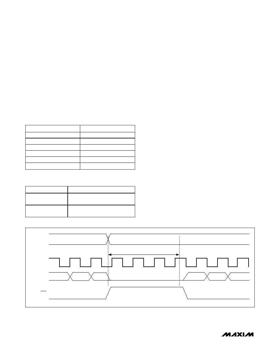
Any spread change causes a delay time of 32,000 x tT
before output data is valid. When the spread amount is
changed from ±2% to ±4% or vice versa, the data out-
puts go low for one tΔSSPLL delay (see Figure 17). The
data outputs stay low, but are not valid when the
spread amount is changed.
Output Enable (OUTEN) and
Busing Outputs
The outputs of two MAX9250s can be bused to form a
2:1 mux with the outputs controlled by the output
enable. Wait 30ns between disabling one deserializer
(driving OUTEN low) and enabling the second one (dri-
ving OUTEN high) to avoid contention of the bused out-
puts. OUTEN controls all outputs except LOCK.
Rising or Falling Output Latch Edge (R/F)
The MAX9248/MAX9250 have a selectable rising or
falling output latch edge through a logic setting on R/F.
Driving R/F high selects the rising output latch edge,
which latches the parallel output data into the next chip
on the rising edge of PCLK_OUT. Driving R/F low
selects the falling output latch edge, which latches the
parallel output data into the next chip on the falling
edge of PCLK_OUT. The MAX9248/MAX9250 output-
latch-edge polarity does not need to match the
MAX9247 serializer input-latch-edge polarity. Select the
latch-edge polarity required by the chip being driven
by the MAX9248/MAX9250.
tΔSSPLL (32,800 x tT)
±4% OR ±2% SPREAD
LOW
SS
PCLK_OUT
RGB_OUT[17:0]
CNTL_OUT8:0]
LOCK
Figure 17. Output Waveforms when Spread Amount is Changed
fPCLK_IN
fM(kHz) = fPCLK_IN / 1024
8
7.81
10
9.77
16
15.63
32
31.25
40
39.06
42
41.01
Table 4. Modulation Rate
SS INPUT LEVEL
OUTPUT SPREAD
High
Data and clock output spread ±4%
relative to REFCLK
Low
Data and clock output spread ±2%
relative to REFCLK
Table 5. SS Function
相關(guān)PDF資料 |
PDF描述 |
|---|---|
| MAX9247GCM+T | IC SERIALIZER LVDS 48-LQFP |
| D38999/24FG41SB | CONN RCPT 41POS JAM NUT W/SCKT |
| D38999/26FE99SA | CONN PLUG 23POS STRAIGHT W/SCKT |
| R5F100MLAFB#V0 | MCU 16BIT 512KB FLASH 80LQFP |
| D38999/26ME26HN | CONN PLUG 26POS STRAIGHT W/PINS |
相關(guān)代理商/技術(shù)參數(shù) |
參數(shù)描述 |
|---|---|
| MAX9251 | 功能描述:串行器/解串器 - Serdes RoHS:否 制造商:Texas Instruments 類型:Deserializer 數(shù)據(jù)速率:1.485 Gbit/s 輸入類型:ECL/LVDS 輸出類型:LVCMOS 輸入端數(shù)量:1 輸出端數(shù)量:20 工作電源電壓:2.375 V to 2.625 V 工作溫度范圍:0 C to + 70 C 封裝 / 箱體:TQFP-64 |
| MAX9252 | 功能描述:串行器/解串器 - Serdes RoHS:否 制造商:Texas Instruments 類型:Deserializer 數(shù)據(jù)速率:1.485 Gbit/s 輸入類型:ECL/LVDS 輸出類型:LVCMOS 輸入端數(shù)量:1 輸出端數(shù)量:20 工作電源電壓:2.375 V to 2.625 V 工作溫度范圍:0 C to + 70 C 封裝 / 箱體:TQFP-64 |
| MAX9253 | 功能描述:串行器/解串器 - Serdes RoHS:否 制造商:Texas Instruments 類型:Deserializer 數(shù)據(jù)速率:1.485 Gbit/s 輸入類型:ECL/LVDS 輸出類型:LVCMOS 輸入端數(shù)量:1 輸出端數(shù)量:20 工作電源電壓:2.375 V to 2.625 V 工作溫度范圍:0 C to + 70 C 封裝 / 箱體:TQFP-64 |
| MAX9254 | 制造商:MAXIM 制造商全稱:Maxim Integrated Products 功能描述:21-Bit Deserializers with Programmable Spread Spectrum and DC Balance |
| MAX9254EUM | 制造商:MAXIM 制造商全稱:Maxim Integrated Products 功能描述:21-Bit Deserializers with Programmable Spread Spectrum and DC Balance |
發(fā)布緊急采購,3分鐘左右您將得到回復(fù)。