- 您現(xiàn)在的位置:買賣IC網(wǎng) > PDF目錄11618 > MAX9175EUB+ (Maxim Integrated Products)SEMICONDUCTOR OTHER PDF資料下載
參數(shù)資料
| 型號: | MAX9175EUB+ |
| 廠商: | Maxim Integrated Products |
| 文件頁數(shù): | 13/14頁 |
| 文件大小: | 0K |
| 描述: | SEMICONDUCTOR OTHER |
| 標準包裝: | 50 |
| 系列: | * |
MAX9174/MAX9175
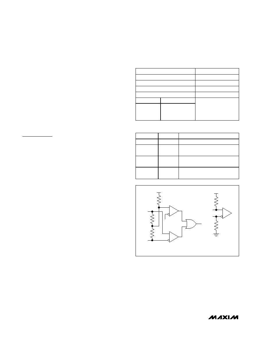
When the input is driven with a differential signal of |VID|
= 50mV to 1.2V within a voltage range of 0 to 2.4V, the
fail-safe circuit is not activated. If the input is open,
undriven and shorted, or undriven and terminated, an
internal resistor in the fail-safe circuit pulls the input
above VCC - 0.3V, activating the fail-safe circuit and
forcing the outputs high (Figure 1).
Overshoot and Undershoot Voltage
Protection
The MAX9174/MAX9175 are designed to protect the
power-down inputs (PD0 and PD1) against latchup due
to transient overshoot and undershoot voltage. If the
input voltage goes above VCC or below GND by up to
1V, an internal circuit limits input current to 1.5mA.
Applications Information
Power-Supply Bypassing
Bypass the VCC pin with high-frequency surface-mount
ceramic 0.1F and 0.001F capacitors in parallel as
close to the device as possible, with the smaller valued
capacitor closest to VCC.
Differential Traces
Input and output trace characteristics affect the perfor-
mance of the MAX9174/MAX9175. Use controlled-
impedance differential traces (100 typ). To reduce
radiated noise and ensure that noise couples as com-
mon mode, route the differential input and output sig-
nals within a pair close together. Reduce skew by
matching the electrical length of the two signal paths
that make up the differential pair. Excessive skew can
result in a degradation of magnetic field cancellation.
Maintain a constant distance between the differential
traces to avoid discontinuities in differential impedance.
Minimize the number of vias to further prevent imped-
ance discontinuities.
Cables and Connectors
Interconnect for LVDS typically has a controlled differ-
ential impedance of 100. Use cables and connectors
that have matched differential impedance to minimize
impedance discontinuities.
Avoid the use of unbalanced cables such as ribbon or
simple coaxial cable. Balanced cables such as twisted
pair offer superior signal quality and tend to generate
less EMI due to magnetic field canceling effects.
Balanced cables pick up noise as common mode,
which is rejected by the LVDS receiver.
Termination
The MAX9174/MAX9175 require external input and out-
put termination resistors. For LVDS, connect an input
termination resistor across the differential input and at
the far end of the interconnect driven by the LVDS out-
puts. Place the input termination resistor as close to the
receiver input as possible. Termination resistors should
match the differential impedance of the transmission
line. Use 1% surface-mount resistors.
670MHz LVDS-to-LVDS and Anything-to-LVDS
1:2 Splitters
8
_______________________________________________________________________________________
INPUT
OUTPUTS
(IN+) - (IN-)
(OUT_+) - (OUT_-)
≥ +50mV
H
≤ -50mV
L
-50mV < VID < +50mV
Indeterminate
MAX9175
Open
MAX9174
Open, undriven
short, or undriven
parallel termination
H
Table 1. Input Function Table
P
PD
D
D11
1
P
PD
D
D00
0
OUT_+, OUT_-
HH
Both outputs enabled
L or open
Shutdown to minimum power,
outputs high impedance to ground
L or open
High
OUT0 enabled, OUT1 high
impedance to ground
High
L or open
OUT1 enabled, OUT0 high
impedance to ground
Table 2. Power-Down Function Table
IN+
TO
OUTPUT
IN-
IN+
IN-
MAX9175 INPUT
MAX9174 INTERNAL FAIL-SAFE CIRCUIT
DIFFERENTIAL
RCVR
COMPARATOR
RIN3
VCC - 0.3V
VCC
RIN2
RIN1
VCC
Figure 1. Input Structure
相關PDF資料 |
PDF描述 |
|---|---|
| VI-J6Z-IW-F3 | CONVERTER MOD DC/DC 2V 40W |
| VI-J6Z-IW-F2 | CONVERTER MOD DC/DC 2V 40W |
| VI-J6Z-IW-F1 | CONVERTER MOD DC/DC 2V 40W |
| D38999/26KE26SN | CONN PLUG 26POS STRAIGHT W/SCKT |
| VI-J6Y-IY-F4 | CONVERTER MOD DC/DC 3.3V 33W |
相關代理商/技術參數(shù) |
參數(shù)描述 |
|---|---|
| MAX9175EUB/GG8 | 制造商:Maxim Integrated Products 功能描述: |
| MAX9175EUB+ | 功能描述:LVDS 接口集成電路 670MHz LVDS->LVDS & X->LVDS 1:2 Splitter RoHS:否 制造商:Texas Instruments 激勵器數(shù)量:4 接收機數(shù)量:4 數(shù)據(jù)速率:155.5 Mbps 工作電源電壓:5 V 最大功率耗散:1025 mW 最大工作溫度:+ 85 C 封裝 / 箱體:SOIC-16 Narrow 封裝:Reel |
| MAX9175EUB+T | 功能描述:LVDS 接口集成電路 670MHz LVDS->LVDS & X->LVDS 1:2 Splitter RoHS:否 制造商:Texas Instruments 激勵器數(shù)量:4 接收機數(shù)量:4 數(shù)據(jù)速率:155.5 Mbps 工作電源電壓:5 V 最大功率耗散:1025 mW 最大工作溫度:+ 85 C 封裝 / 箱體:SOIC-16 Narrow 封裝:Reel |
| MAX9175EUB-T | 制造商:Maxim Integrated Products 功能描述:670MHZ LVDS-TO-LVDS AND ANYTHING -TO-LVDS 1:2 - Tape and Reel |
| MAX9176 | 制造商:MAXIM 制造商全稱:Maxim Integrated Products 功能描述:670MHz LVDS-to-LVDS and Anything-to-LVDS 2:1 Multiplexers |
發(fā)布緊急采購,3分鐘左右您將得到回復。