- 您現(xiàn)在的位置:買賣IC網(wǎng) > PDF目錄384710 > MAX886 (Maxim Integrated Products, Inc.) Octal Transparent D-type Latches With 3-State Outputs 20-CDIP -55 to 125 PDF資料下載
參數(shù)資料
| 型號: | MAX886 |
| 廠商: | Maxim Integrated Products, Inc. |
| 英文描述: | Octal Transparent D-type Latches With 3-State Outputs 20-CDIP -55 to 125 |
| 中文描述: | 無線和衛(wèi)星手機電源管理IC |
| 文件頁數(shù): | 2/20頁 |
| 文件大?。?/td> | 257K |
| 代理商: | MAX886 |
M
Wireless and S atellite Handset
Power-Management ICs
2
_______________________________________________________________________________________
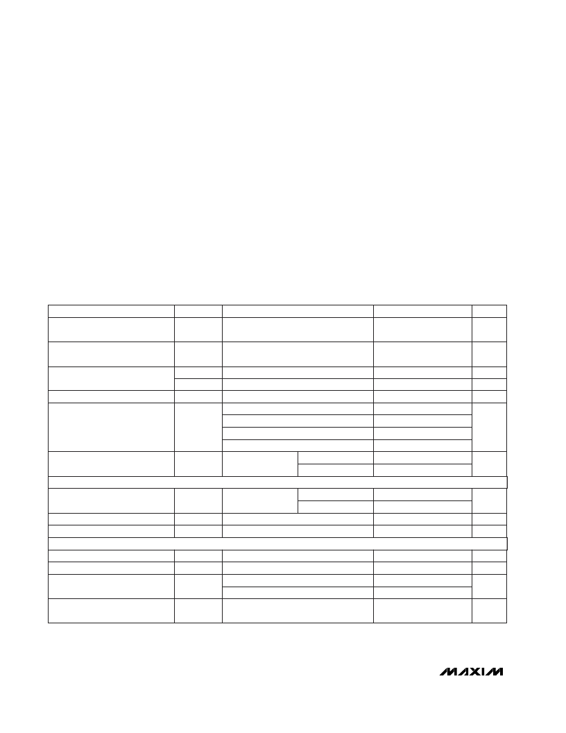
ABSOLUTE MAXIMUM RATINGS
BATT, IN0, IN1 to GND...........................................-0.3V to +13V
CVH to IN0................................................................-6V to +0.3V
PGND, DGND to GND...........................................-0.3V to +0.3V
ONSTAT to GND.....................................-0.3V to (V
OUT2
+ 0.3V)
LX to PGND.............................................-0.3V to (V
OUT0
+ 0.3V)
OUT1 to GND.............................................-0.3V to (V
IN1
+ 0.3V)
OUT2 to GND.............................................-0.3V to (V
IN2
+ 0.3V)
OUT3 to GND.............................................-0.3V to (V
IN3
+ 0.3V)
OUT5 to GND.............................................-0.3V to (V
IN5
+ 0.3V)
ELECTRICAL CHARACTERISTICS
(V
BATT
= V
IN0
= V
IN1
= +5.5V, GND = PGND = DGND, V
OFF
= V
SYNC
= 2.8V, V
IN2
= V
IN3
= V
IN4
= V
IN5
= +3.8V, V
OUT4
= +5.5V,
T
A
= -40°C to +85°C, unless otherwise noted. Typical values are at T
A
= +25°C.) (Note 1)
Stresses beyond those listed under “Absolute Maximum Ratings” may cause permanent damage to the device. These are stress ratings only, and functional
operation of the device at these or any other conditions beyond those indicated in the operational sections of the specifications is not implied. Exposure to
absolute maximum rating conditions for extended periods may affect device reliability.
SYNC,
RESET
, SCL, SDA, CVL, LBI, LBHYS, OUT0
REF,
LBO
, C+, C-, OUT4, IN2, IN3, IN4, IN5,
ON
,
OFF
to GND ...................................................-0.3V to +6V
Continuous Power Dissipation (T
A
= +70°C)
TQFP (derate 11.1mW/°C above +70°C)......................889mW
Operating Temperature Range. ......................... -40°C to +85°C
J unction Temperature......................................................+150°C
Storage Temperature Range.............................-65°C to +150°C
Lead Temperature (soldering, 10sec) .............................+300°C
V
OUT0
= 3.75V (MAX886),
V
OUT0
= 2.027V (MAX888)
MAX888
MAX886
I
OUT0
= 0
2.7V < V
OUT0
< 3.75V
f
OSC
= 375kHz
f
OSC
= 535kHz
f
OSC
= 670kHz
f
OSC
= 925kHz
1μA < I
REF
< 100μA
I
REF
= 0
SYNC = GND
V
BATT
falling
V
BATT
rising
CONDITIONS
% of
V
OUT0
Output Ready Threshold
-7.5
-5
-3
V
1.527
3.027
V
OUT0
Nominal Output Adjustment
Range
2.625
3.750
%
-3
3
Output Accuracy
V
2.7
12
V
IN0
Input Voltage Range
mV
0.2
5
Reference Supply Rejection
DC-DC BUCK REGULATOR 0 (IN0, OUT0)
mV
5
15
Reference Load Regulation
V
1.225
1.275
V
REF
Reference Output Voltage
1.23
1.25
1.27
V
2.7
5.5
V
IN2
, V
IN3
,
V
IN4
, V
IN5
IN2, IN3, IN4, IN5 Operating
Voltage Range
V
2.7
12
V
BATT
, V
IN0
,
V
IN1
BATT, IN0, IN1 Operating Voltage
Range
5
10
15
2
3
4
μA
250
600
I
BATTPFM
Supply Current, PFM Mode
V
V
2.35
2.45
2.55
V
UVLOF
V
UVLOR
2.65
Undervoltage Lockout
UNITS
MIN
TYP
MAX
SYMBOL
PARAMETER
OFF
= GND
μA
I
STNBY
Supply Current, Shutdown Mode
T
A
= 0°C to +85°C
T
A
= -40°C to +85°C
T
A
= 0°C to +85°C
T
A
= -40°C to +85°C
mA
5.5
12
I
BATTPWM
Supply Current, PWM Mode
REFERENCE
相關PDF資料 |
PDF描述 |
|---|---|
| MAX8868 | Low-Noise, Low-Dropout, 150mA Linear Regulators in SOT23 |
| MAX8867 | Low-Noise, Low-Dropout, 150mA Linear Regulators in SOT23 |
| MAX886_EUK25 | Low-Noise, Low-Dropout, 150mA Linear Regulators in SOT23 |
| MAX886_EUK28 | Low-Noise, Low-Dropout, 150mA Linear Regulators in SOT23 |
| MAX886_EUK29 | Octal Edge-Triggered D-type Flip-Flops With 3-State Outputs 20-CDIP -55 to 125 |
相關代理商/技術參數(shù) |
參數(shù)描述 |
|---|---|
| MAX8860ESA33 | 制造商:Rochester Electronics LLC 功能描述: 制造商:Maxim Integrated Products 功能描述: |
| MAX8860ESA33.TG002 | 制造商:Rochester Electronics LLC 功能描述: 制造商:Maxim Integrated Products 功能描述: |
| MAX8860ESA33-T | 制造商:Rochester Electronics LLC 功能描述: 制造商:Maxim Integrated Products 功能描述: |
| MAX8860EUA18 | 功能描述:低壓差穩(wěn)壓器 - LDO 300mA Linear Regulator RoHS:否 制造商:Texas Instruments 最大輸入電壓:36 V 輸出電壓:1.4 V to 20.5 V 回動電壓(最大值):307 mV 輸出電流:1 A 負載調(diào)節(jié):0.3 % 輸出端數(shù)量: 輸出類型:Fixed 最大工作溫度:+ 125 C 安裝風格:SMD/SMT 封裝 / 箱體:VQFN-20 |
| MAX8860EUA18+ | 功能描述:低壓差穩(wěn)壓器 - LDO 300mA Linear Regulator RoHS:否 制造商:Texas Instruments 最大輸入電壓:36 V 輸出電壓:1.4 V to 20.5 V 回動電壓(最大值):307 mV 輸出電流:1 A 負載調(diào)節(jié):0.3 % 輸出端數(shù)量: 輸出類型:Fixed 最大工作溫度:+ 125 C 安裝風格:SMD/SMT 封裝 / 箱體:VQFN-20 |
發(fā)布緊急采購,3分鐘左右您將得到回復。