- 您現(xiàn)在的位置:買賣IC網(wǎng) > PDF目錄385550 > MAX783 (Maxim Integrated Products, Inc.) Triple-Output Power-Supply Controller for Notebook Computers(3.3V/5V,具有雙組PCMCIA標(biāo)準(zhǔn)VPP輸出的筆記本電腦電源控制器) PDF資料下載
參數(shù)資料
| 型號: | MAX783 |
| 廠商: | Maxim Integrated Products, Inc. |
| 英文描述: | Triple-Output Power-Supply Controller for Notebook Computers(3.3V/5V,具有雙組PCMCIA標(biāo)準(zhǔn)VPP輸出的筆記本電腦電源控制器) |
| 中文描述: | 三輸出電源控制器,用于筆記本電腦 |
| 文件頁數(shù): | 2/28頁 |
| 文件大?。?/td> | 327K |
| 代理商: | MAX783 |
第1頁當(dāng)前第2頁第3頁第4頁第5頁第6頁第7頁第8頁第9頁第10頁第11頁第12頁第13頁第14頁第15頁第16頁第17頁第18頁第19頁第20頁第21頁第22頁第23頁第24頁第25頁第26頁第27頁第28頁
M
Triple-Output Power-S upply Controller
for Notebook Computers
2
_______________________________________________________________________________________
V+ to GND.................................................................-0.3V, +36V
PGND to GND........................................................................±2V
VL to GND ...................................................................-0.3V, +7V
BST3, BST5 to GND ..................................................-0.3V, +36V
LX3 to BST3.................................................................-7V, +0.3V
LX5 to BST5.................................................................-7V, +0.3V
In(D1, D2, S———N, ON5, REF, SYNC, DA1, DA0, DB1, DB0, ON5,
SS5, CS5, FB5, R———, CS3, FB3, SS3, ON3).-0.3V, (VL + 0.3V)
VDD to GND.................................................................-0.3V, 20V
VPPA, VPPB to GND.....................................-0.3V, (VDD + 0.3V)
VH to GND ...................................................................-0.3V, 20V
Q1, Q2 to GND................................................-0.3V, (VH + 0.3V)
DL3, DL5 to PGND..........................................-0.3V , (VL + 0.3V)
DH3 to LX3..................................................-0.3V, (BST3 + 0.3V)
DH5 to LX5..................................................-0.3V, (BST5 + 0.3V)
REF, VL, VPP Short to GND........................................Momentary
REF Current.........................................................................20mA
VL Current...........................................................................50mA
VPPA, VPPB Current.........................................................100mA
Continuous Power Dissipation (T
A
= +70°C)
SSOP (derate 11.76mW/°C above +70°C) ...................762mW
Operating Temperature Ranges:
MAX783CBX/MAX783_CBX.................................0°C to +70°C
MAX783EBX/MAX783_EBX ..............................-40°C to +85°C
Storage Temperature Range.............................-65°C to +160°C
Lead Temperature (soldering, 10sec) .............................+300°C
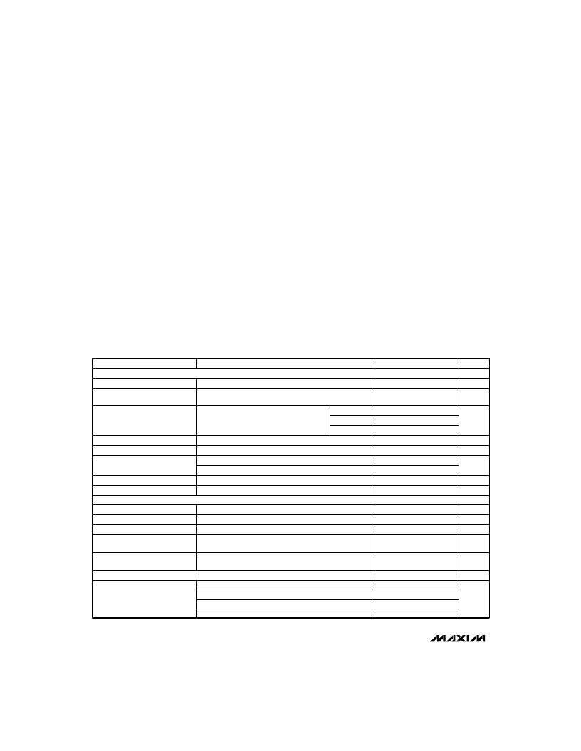
ELECTRICAL CHARACTERISTICS
(V+ = 15V, GND = PGND = 0V, I
VL
= I
REF
= 0mA, S—H—D—N= ON3 = ON5 = 5V, other digital input levels are 0V or +5V,
T
A
= T
MIN
to T
MAX
, unless otherwise noted.)
Stresses beyond those listed under “Absolute Maximum Ratings” may cause permanent damage to the device. These are stress ratings only, and functional
operation of the device at these or any other conditions beyond those indicated in the operational sections of the specifications is not implied. Exposure to
absolute maximum rating conditions for extended periods may affect device reliability.
ABSOLUTE MAXIMUM RATINGS
VDD = 18V, ON3 = ON5 = 5V, VPPA/VPPB programmed to
0V
0mV < (CS5-FB5) < 70mV, 6V < V + < 30V
(includes load and line regulation)
Program to 0V, 13V < VDD < 19V, 0mA < I
L
< 0.3mA
Program to 3.3V, 13V < VDD < 19V, 0mA < I
L
< 60mA
Program to 5V, 13V < VDD < 19V, 0mA < I
L
< 60mA
Program to 12V, 13V < VDD < 19V, 0mA < I
L
< 60mA
VDD = 18V, ON3 = ON5 = 5V, VPPA/VPPB programmed to
12V with no external load
VDD = 20V
CS3-FB3 (VDD < 13V, flyback mode)
Either controller (0mV to 70mV)
Either controller (6V to 30V)
CS3-FB3 or CS5-FB5
Rising edge, hysteresis = 1%
Falling edge, hysteresis = 1%
CONDITIONS
V
4.80
5.08
5.20
-0.30
0.30
FB5 Output Voltage
3.17
3.30
3.43
V
5.5
30
4.85
5.05
5.20
V
11.60
12.10
12.50
VPPA/VPPB Output Voltage
Input Supply Range
μA
15
30
Off VDD Current
μA
mA
140
300
2
SS3/SS5 Fault Sink Current
15V FLYBACK CONTROLLER
Quiescent VDD Current
mA
2
3
μA
2.5
4.0
6.5
SS3/SS5 Source Current
-50
-100
-160
VDD Shunt Current
%
V
2.5
0.03
100
Load Regulation
Line Regulation
%/V
18
20
mV
VDD Shunt Setpoint
80
120
V
Current-Limit Voltage
UNITS
13
14
MIN
TYP
MAX
VDD Regulation Setpoint
PARAMETER
3.17
3.32
3.46
3.35
3.50
3.65
3.46
3.60
3.75
0mV < (CS3-FB3) < 70mV, 6V < V + < 30V
(includes load and line regulation)
V
FB3 Output Voltage
MAX783
MAX783R
MAX783S
3.3V AND 5V STEP-DOWN CONTROLLERS
PCMCIA REGULATORS (Note 1)
相關(guān)PDF資料 |
PDF描述 |
|---|---|
| MAX786 | Dual-Output Power-Supply Controller for Notebook Computers(具有25μA關(guān)斷的,3.3V/5V筆記本型電腦電源) |
| MAX787 | 5V/3.3V/3V 5A Step-Down, PWM, Switch-Mode DC-DC Regulators(5A,5V步降,PWM,開關(guān)型DC-DC變換器) |
| MAX788 | 5V/3.3V/3V 5A Step-Down, PWM, Switch-Mode DC-DC Regulators(5A,5V步降,PWM,開關(guān)型DC-DC變換器) |
| MAX789 | 5V/3.3V/3V 5A Step-Down, PWM, Switch-Mode DC-DC Regulators(5A,5V步降,PWM,開關(guān)型DC-DC變換器) |
| MAX791 | Microprocessor Supervisory Circuit(微處理器監(jiān)控電路) |
相關(guān)代理商/技術(shù)參數(shù) |
參數(shù)描述 |
|---|---|
| MAX783CBX | 功能描述:DC/DC 開關(guān)控制器 RoHS:否 制造商:Texas Instruments 輸入電壓:6 V to 100 V 開關(guān)頻率: 輸出電壓:1.215 V to 80 V 輸出電流:3.5 A 輸出端數(shù)量:1 最大工作溫度:+ 125 C 安裝風(fēng)格: 封裝 / 箱體:CPAK |
| MAX783CBX-T | 功能描述:DC/DC 開關(guān)控制器 RoHS:否 制造商:Texas Instruments 輸入電壓:6 V to 100 V 開關(guān)頻率: 輸出電壓:1.215 V to 80 V 輸出電流:3.5 A 輸出端數(shù)量:1 最大工作溫度:+ 125 C 安裝風(fēng)格: 封裝 / 箱體:CPAK |
| MAX783EBX | 功能描述:DC/DC 開關(guān)控制器 RoHS:否 制造商:Texas Instruments 輸入電壓:6 V to 100 V 開關(guān)頻率: 輸出電壓:1.215 V to 80 V 輸出電流:3.5 A 輸出端數(shù)量:1 最大工作溫度:+ 125 C 安裝風(fēng)格: 封裝 / 箱體:CPAK |
| MAX783EBX+ | 功能描述:DC/DC 開關(guān)控制器 RoHS:否 制造商:Texas Instruments 輸入電壓:6 V to 100 V 開關(guān)頻率: 輸出電壓:1.215 V to 80 V 輸出電流:3.5 A 輸出端數(shù)量:1 最大工作溫度:+ 125 C 安裝風(fēng)格: 封裝 / 箱體:CPAK |
| MAX783EBX+T | 功能描述:DC/DC 開關(guān)控制器 RoHS:否 制造商:Texas Instruments 輸入電壓:6 V to 100 V 開關(guān)頻率: 輸出電壓:1.215 V to 80 V 輸出電流:3.5 A 輸出端數(shù)量:1 最大工作溫度:+ 125 C 安裝風(fēng)格: 封裝 / 箱體:CPAK |
發(fā)布緊急采購,3分鐘左右您將得到回復(fù)。