- 您現(xiàn)在的位置:買(mǎi)賣(mài)IC網(wǎng) > PDF目錄11019 > MAX7413CUA+T (Maxim Integrated Products)IC FILTER LOWPASS 5TH 8UMAX PDF資料下載
MAX7409/MAX7410/MAX7413/MAX7414
5th-Order, Lowpass,
Switched-Capacitor Filters
2
_______________________________________________________________________________________
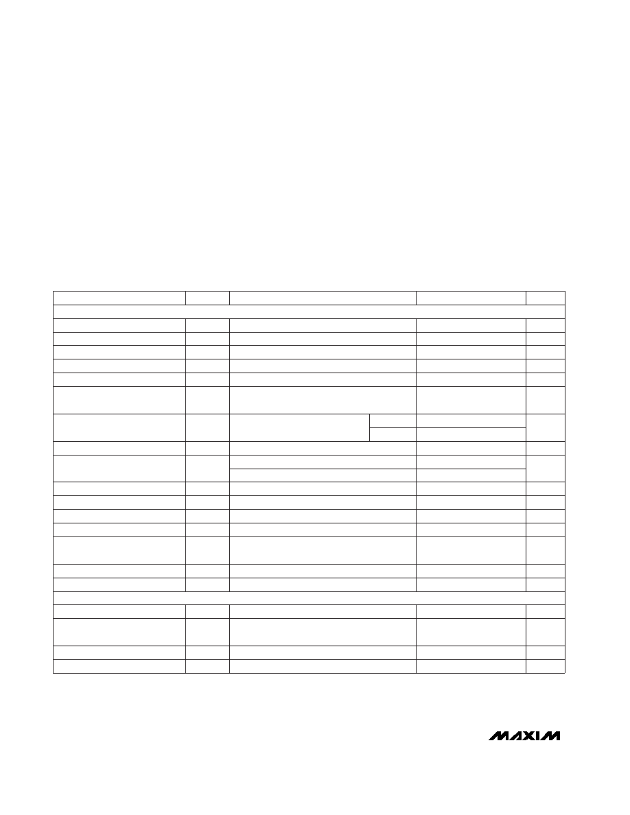
ABSOLUTE MAXIMUM RATINGS
ELECTRICAL CHARACTERISTICS—MAX7409/MAX7410
(VDD = +5V, filter output measured at OUT, 10k || 50pF load to GND at OUT, OS = COM, 0.1F capacitor from COM to GND,
SHDN = VDD, fCLK = 100kHz, TA = TMIN to TMAX, unless otherwise noted. Typical values are at TA = +25°C.)
Stresses beyond those listed under “Absolute Maximum Ratings” may cause permanent damage to the device. These are stress ratings only, and functional
operation of the device at these or any other conditions beyond those indicated in the operational sections of the specifications is not implied. Exposure to
absolute maximum rating conditions for extended periods may affect device reliability.
VDD to GND ..............................................................-0.3V to +6V
IN, OUT, COM, OS, CLK, SHDN ................-0.3V to (VDD + 0.3V)
OUT Short-Circuit Duration...................................................1sec
Continuous Power Dissipation (TA = +70°C)
8-Pin DIP (derate 9.09mW/°C above +70°C) ...............727mW
8-Pin MAX (derate 4.1mW/°C above +70°C) .............330mW
Operating Temperature Ranges
MAX74 _ _C_A ...................................................0°C to +70°C
MAX74 _ _E_A ................................................-40°C to +85°C
Storage Temperature Range .............................-65°C to +160°C
Lead Temperature (soldering, 10sec) .............................+300°C
COSC = 1000pF (Note 3)
VOS = 0 to VDD
SHDN = GND, VCOM = 0 to VDD
(Note 1)
Input, COM externally driven
OS to OUT
Input, OS externally driven
fIN = 200Hz, VIN = 4Vp-p,
measurement bandwidth = 22kHz
VIN = VCOM = VDD / 2
VCOM = VDD / 2 (Note 2)
Output, COM unconnected
CONDITIONS
21
30
38
fOSC
Internal Oscillator Frequency
±0.1
±10
Input Leakage Current at OS
±0.1
±10
Input Leakage Current at COM
50
500
CL
10
1
RL
Resistive Output Load Drive
5
Clock Feedthrough
110
180
RCOM
Input Resistance at COM
VCOM ±0.1
VOS
2.3
2.5
2.7
100:1
fCLK / fc
Clock-to-Corner Ratio
0.001 to 15
fc
Corner Frequency
VCOM
1
AOS
Offset Voltage Gain
-85
THD+N
Total Harmonic Distortion
plus Noise
10
Clock-to-Corner Tempco
0.25
VDD - 0.25
Output Voltage Range
±4
±25
VOFFSET
Output Offset Voltage
-0.2
0
0.2
DC Insertion Gain with
Output Offset Removed
MIN
TYP
MAX
SYMBOL
PARAMETER
VCLK = 0 or 5V
0.5
VIL
Clock Input Low
4.5
VIH
Clock Input High
±13.5
±20
ICLK
Clock Output Current
(Internal Oscillator Mode)
V
A
kHz
A
pF
k
mVp-p
k
V
V/V
dB
mV
V
ppm/°C
kHz
UNITS
Maximum Capacitive Output
Load Drive
FILTER CHARACTERISTICS
CLOCK
MAX7409
MAX7410
-78
COM Voltage Range
2.0
2.5
3.0
Input Voltage Range at OS
相關(guān)PDF資料 |
PDF描述 |
|---|---|
| VE-20N-IY-F4 | CONVERTER MOD DC/DC 18.5V 50W |
| VE-21Y-IY-F2 | CONVERTER MOD DC/DC 3.3V 33W |
| VE-21Y-IY-F1 | CONVERTER MOD DC/DC 3.3V 33W |
| VE-21Y-IX-F4 | CONVERTER MOD DC/DC 3.3V 49.5W |
| VE-21Y-IX-F2 | CONVERTER MOD DC/DC 3.3V 49.5W |
相關(guān)代理商/技術(shù)參數(shù) |
參數(shù)描述 |
|---|---|
| MAX7413EPA | 功能描述:有源濾波器 RoHS:否 制造商:Maxim Integrated 通道數(shù)量:1 截止頻率:150 KHz 電源電壓-最大:11 V 電源電壓-最小:4.74 V 最大工作溫度:+ 85 C 安裝風(fēng)格:Through Hole 封裝 / 箱體:PDIP N 封裝:Tube |
| MAX7413EPA+ | 功能描述:有源濾波器 5th-Order Lowpass Elliptic Filter RoHS:否 制造商:Maxim Integrated 通道數(shù)量:1 截止頻率:150 KHz 電源電壓-最大:11 V 電源電壓-最小:4.74 V 最大工作溫度:+ 85 C 安裝風(fēng)格:Through Hole 封裝 / 箱體:PDIP N 封裝:Tube |
| MAX7413EUA | 功能描述:有源濾波器 RoHS:否 制造商:Maxim Integrated 通道數(shù)量:1 截止頻率:150 KHz 電源電壓-最大:11 V 電源電壓-最小:4.74 V 最大工作溫度:+ 85 C 安裝風(fēng)格:Through Hole 封裝 / 箱體:PDIP N 封裝:Tube |
| MAX7413EUA+ | 功能描述:有源濾波器 5th-Order Lowpass Elliptic Filter RoHS:否 制造商:Maxim Integrated 通道數(shù)量:1 截止頻率:150 KHz 電源電壓-最大:11 V 電源電壓-最小:4.74 V 最大工作溫度:+ 85 C 安裝風(fēng)格:Through Hole 封裝 / 箱體:PDIP N 封裝:Tube |
| MAX7413EUA+T | 功能描述:有源濾波器 5th-Order Lowpass Elliptic Filter RoHS:否 制造商:Maxim Integrated 通道數(shù)量:1 截止頻率:150 KHz 電源電壓-最大:11 V 電源電壓-最小:4.74 V 最大工作溫度:+ 85 C 安裝風(fēng)格:Through Hole 封裝 / 箱體:PDIP N 封裝:Tube |
發(fā)布緊急采購(gòu),3分鐘左右您將得到回復(fù)。