- 您現(xiàn)在的位置:買賣IC網(wǎng) > PDF目錄383442 > MAX5732AETN (MAXIM INTEGRATED PRODUCTS INC) 32-Channel, 16-Bit, Voltage-Output DACs with Serial Interface PDF資料下載
參數(shù)資料
| 型號: | MAX5732AETN |
| 廠商: | MAXIM INTEGRATED PRODUCTS INC |
| 元件分類: | DAC |
| 英文描述: | 32-Channel, 16-Bit, Voltage-Output DACs with Serial Interface |
| 中文描述: | SERIAL INPUT LOADING, 20 us SETTLING TIME, 16-BIT DAC, QCC56 |
| 封裝: | 8 X 8 MM, 0.80 MM HEIGHT, MO-220, QFN-56 |
| 文件頁數(shù): | 17/26頁 |
| 文件大?。?/td> | 451K |
| 代理商: | MAX5732AETN |
第1頁第2頁第3頁第4頁第5頁第6頁第7頁第8頁第9頁第10頁第11頁第12頁第13頁第14頁第15頁第16頁當(dāng)前第17頁第18頁第19頁第20頁第21頁第22頁第23頁第24頁第25頁第26頁
M
32-Channel, 16-Bit, Voltage-Output
DACs with Serial Interface
______________________________________________________________________________________
17
it is the offset DAC that determines the end-point volt-
ages of the range. Table 1 shows the offset DAC code
required during power-up.
Note:
The offset DAC of every device can be pro-
grammed with any of the four output voltage ranges.
However, the specifications in the
Electrical
Characteristics
table are only guaranteed (production
tested) for the offset code associated with each partic-
ular part number. For example, the MAX5734 specifica-
tions are only valid with the MAX5734 offset- DAC code
shown in Table 1.
The offset DAC is summed with GS (Figure 1). The offset
DAC can also cancel the offset of the output buffers.
Any change in the offset DAC affects all 32 DACs.
The offset DAC is also configured identically to the
other 32 DACs with an input and DAC register. Write to
the offset DAC through the serial interface by using
control bits C2, C1, and C0 = 001 followed by the data
bits D15–D0. The
CLR
command affects the offset DAC
as well as the other DACs.
The data format for the offset DAC codes are: control bits
C2, C1, and C0 = 011, address bits A5–A0 = 100000, 7
don’t-care bits, and 16 data bits as shown in Table 2.
Output Amplifiers (OUT0–OUT31)
All DAC outputs are internally buffered. The internal
buffers provide gain, improved load regulation, and tran-
sition glitch suppression for the DAC outputs. The output
buffers slew at 1V/μs and can drive 10k
in parallel with
100pF. The output buffers are powered by AV
CC
and
V
SS
. AV
CC
and V
SS
determine the maximum output
voltage range of the device.
The input code, the voltage reference, the offset DAC
output, the voltage on GS, and the gain of the output
amplifier determine the output voltage. Calculate V
OUT
as follows:
×
(
2
16
where GAIN = 5/3 for the MAX5732, or GAIN = 10/3 for
the MAX5733/MAX5734/MAX5735.
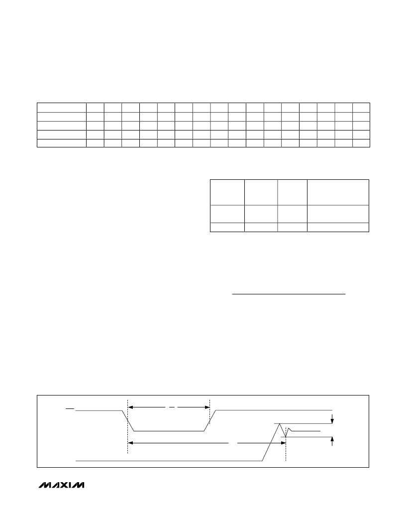
Load-DAC (
LDAC
) Input
The MAX5732–MAX5735 feature an active-low
LDAC
logic input that allows the outputs OUT_ to update
asynchronously. Keep
LDAC
high during normal opera-
tion (when the device is controlled only through the ser-
ial interface). Drive
LDAC
low to simultaneously update
all DAC outputs with data from their respective input
registers. Figure 3 shows the
LDAC
timing with respect
to OUT_.
V
GAIN
V
DAC code
offset DAC code
V
OUT
REF
GS
=
×
)
+
PART NUMBER
MAX5732
MAX5733
MAX5734
MAX5735
D15
0
0
0
1
D14
0
0
1
0
D13
0
0
0
0
D12
0
0
0
0
D11
0
0
0
0
D10
0
0
0
0
D9
0
0
0
0
D8
0
0
0
0
D7
0
0
0
0
D6
0
0
0
0
D5
0
0
0
0
D4
0
0
0
0
D3
0
0
0
0
D2
0
0
0
0
D1
0
0
0
0
D0
0
0
0
0
Table 1. Offset DAC Codes
OUT_
±
0.5 LSB
t
S
t
LDAC
LDAC
Figure 3.
LDAC
Timing
Note:
For the MAX5732, the maximum code for the offset DAC is 16384. For the MAX5733/MAX5734/MAX5735, the maximum code
for the offset DAC is 40000.
Table 2. Serial Data Format
CONTROL
BITS
ADDRESS
BITS
DON’T-
CARE
BITS
DATA BITS
C2, C1,
AND C0
A5–A0
—
D15–D0
011
100000
XXXXXXX
See table 1
相關(guān)PDF資料 |
PDF描述 |
|---|---|
| MAX5732BCTN | 32-Channel, 16-Bit, Voltage-Output DACs with Serial Interface |
| MAX5735CCTN | CONNECTOR |
| MAX5735CETN | CONNECTOR |
| MAX5732BETN | 32-Channel, 16-Bit, Voltage-Output DACs with Serial Interface |
| MAX5733ACTN | 32-Channel, 16-Bit, Voltage-Output DACs with Serial Interface |
相關(guān)代理商/技術(shù)參數(shù) |
參數(shù)描述 |
|---|---|
| MAX5732AETN-T | 制造商:Maxim Integrated Products 功能描述:16-BIT 32 CHANNEL 0 - 5V VOUT DAC - Tape and Reel |
| MAX5732AUCB | 制造商:Maxim Integrated Products 功能描述:16-BIT 32 CHANNEL 0 - 5V VOUT DAC - Rail/Tube |
| MAX5732AUTN | 功能描述:數(shù)模轉(zhuǎn)換器- DAC RoHS:否 制造商:Texas Instruments 轉(zhuǎn)換器數(shù)量:1 DAC 輸出端數(shù)量:1 轉(zhuǎn)換速率:2 MSPs 分辨率:16 bit 接口類型:QSPI, SPI, Serial (3-Wire, Microwire) 穩(wěn)定時間:1 us 最大工作溫度:+ 85 C 安裝風(fēng)格:SMD/SMT 封裝 / 箱體:SOIC-14 封裝:Tube |
| MAX5732AUTN+ | 功能描述:數(shù)模轉(zhuǎn)換器- DAC 10-Bit 32Ch Precision DAC RoHS:否 制造商:Texas Instruments 轉(zhuǎn)換器數(shù)量:1 DAC 輸出端數(shù)量:1 轉(zhuǎn)換速率:2 MSPs 分辨率:16 bit 接口類型:QSPI, SPI, Serial (3-Wire, Microwire) 穩(wěn)定時間:1 us 最大工作溫度:+ 85 C 安裝風(fēng)格:SMD/SMT 封裝 / 箱體:SOIC-14 封裝:Tube |
| MAX5732AUTN+T | 功能描述:數(shù)模轉(zhuǎn)換器- DAC 10-Bit 32Ch Precision DAC RoHS:否 制造商:Texas Instruments 轉(zhuǎn)換器數(shù)量:1 DAC 輸出端數(shù)量:1 轉(zhuǎn)換速率:2 MSPs 分辨率:16 bit 接口類型:QSPI, SPI, Serial (3-Wire, Microwire) 穩(wěn)定時間:1 us 最大工作溫度:+ 85 C 安裝風(fēng)格:SMD/SMT 封裝 / 箱體:SOIC-14 封裝:Tube |
發(fā)布緊急采購,3分鐘左右您將得到回復(fù)。