- 您現(xiàn)在的位置:買賣IC網(wǎng) > PDF目錄384685 > MAX534AMJE (MAXIM INTEGRATED PRODUCTS INC) +5V, Low-Power, 8-Bit Quad DAC with Rail-to-Rail Output Buffers PDF資料下載
參數(shù)資料
| 型號(hào): | MAX534AMJE |
| 廠商: | MAXIM INTEGRATED PRODUCTS INC |
| 元件分類: | DAC |
| 英文描述: | +5V, Low-Power, 8-Bit Quad DAC with Rail-to-Rail Output Buffers |
| 中文描述: | SERIAL INPUT LOADING, 8 us SETTLING TIME, 8-BIT DAC, CDIP16 |
| 封裝: | 0.300 INCH, CERAMIC, DIP-16 |
| 文件頁(yè)數(shù): | 8/16頁(yè) |
| 文件大?。?/td> | 125K |
| 代理商: | MAX534AMJE |
第1頁(yè)第2頁(yè)第3頁(yè)第4頁(yè)第5頁(yè)第6頁(yè)第7頁(yè)當(dāng)前第8頁(yè)第9頁(yè)第10頁(yè)第11頁(yè)第12頁(yè)第13頁(yè)第14頁(yè)第15頁(yè)第16頁(yè)
M
+5V, Low-Power, 8-Bit Quad DAC
with Rail-to-Rail Output Buffers
8
_______________________________________________________________________________________
_______________Detailed Desc ription
S erial Interfac e
At power-on, the serial interface and all digital-to-
analog converters (DACs) are cleared and set to code
zero. The serial data output (DOUT) is set to transition
on SCLK’s falling edge.
The MAX534 communicates with microprocessors
through a synchronous, full-duplex, 3-wire interface
(Figure 1). Data is sent MSB first and can be transmit-
ted in one 4-bit and one 8-bit (byte) packet or in one
12-bit word. If a 16-bit word is used, the first four bits
are ignored. A 4-wire interface adds a line for
LDAC
and allows asynchronous updating. The serial clock
(SCLK) synchronizes the data transfer. Data is transmit-
ted and received simultaneously.
Figure 2 shows the detailed serial-interface timing.
Please note that the clock should be low if it is stopped
between updates. DOUT does not go into a high-
impedance state if the clock idles or
CS
is high.
Serial data is clocked into the data registers in MSB-first
format, with the address and configuration information
preceding the actual DAC data. Data is clocked in on
SCLK’s rising edge while
CS
is low. Data at DOUT is
clocked out 12 clock cycles later, either at SCLK’s falling
edge (default or mode 0) or rising edge (mode 1).
Chip select (
CS
) must be low to enable the DAC. If
CS
is high, the interface is disabled and DOUT remains
unchanged.
CS
must go low at least 40ns before the
first rising edge of the clock pulse to properly clock in
the first bit. With
CS
low, data is clocked into the
MAX534’s internal shift register on the rising edge of
the external serial clock. Always clock in the full 12 bits
because each time
CS
goes high the bits currently in
the input shift register are interpreted as a command.
SCLK can be driven at rates up to 10MHz.
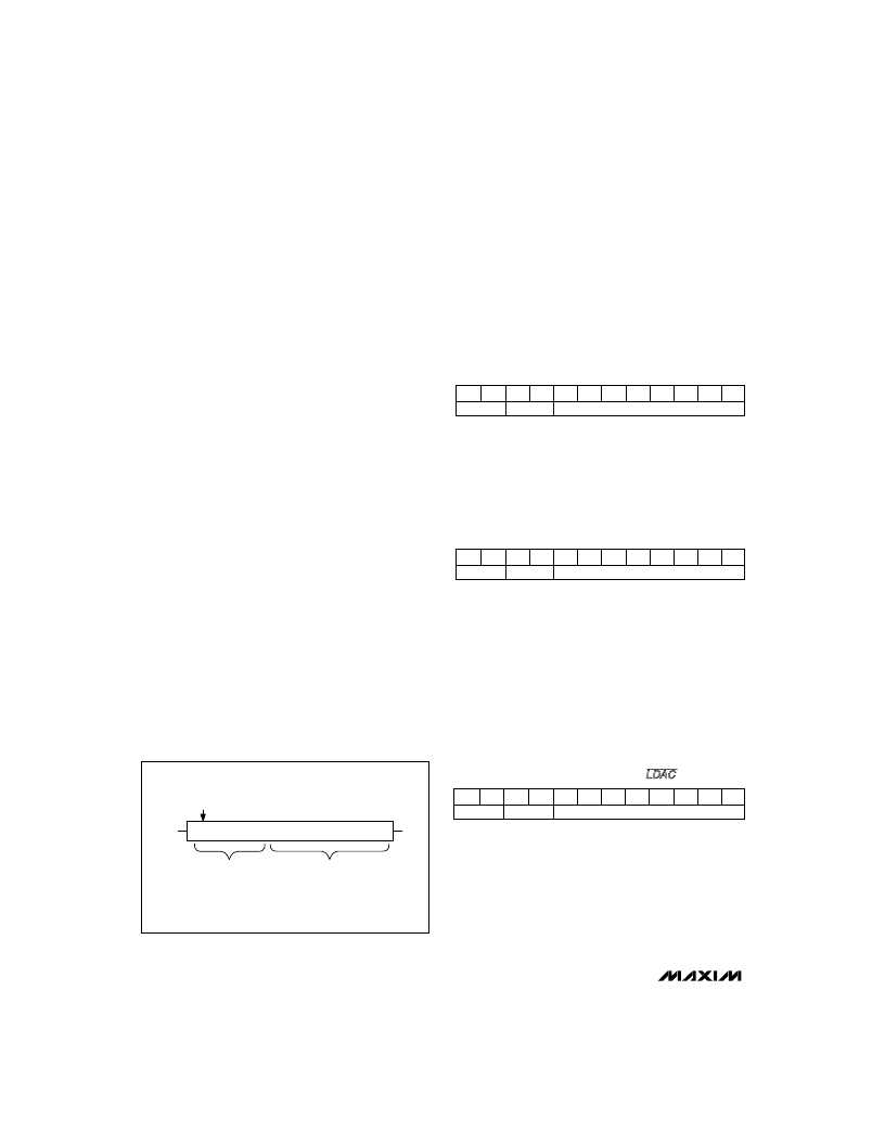
Serial Input Data Format and Control Codes
The 12-bit serial input format shown in Figure 3 com-
prises two DAC address bits (A1, A0), two control bits
(C1, C0), and eight bits of data (D7...D0).
The 4-bit address/control code configures the DAC as
shown in Table 1.
Load Input Register, DAC Registers Unchanged
(Single Update Operation)
When performing a single update operation, A1 and A0
select the respective input register. At the rising edge
of
CS
, the selected input register is loaded with the cur-
rent shift-register data. All DAC outputs remain
unchanged. This preloads individual data in the input
register without changing the DAC outputs.
Load Input and DAC Registers
This command directly loads the selected DAC register
at
CS
’s rising edge. A1 and A0 set the DAC address.
Current shift-register data is placed in the selected
input and DAC registers.
For example, to load all four DAC registers simultaneously
with individual settings (DAC A = 1V, DAC B = 2V,
DAC C = 3V, and DAC D = 4V), four commands are
required. First, perform three single input register
update operations for DACs A, B, and C (C1 = 0). The
final command loads input register D and updates all
four DAC registers from their respective input registers.
Software “
LDAC
” Command
When this command is initiated, all DAC registers are
updated with the contents of their respective input reg-
isters at
CS
’s rising edge. With the exception of using
CS
to execute, this performs the same function as the
asynchronous
LDAC.
Figure 3. Serial Input Format
THIS IS THE FIRST BIT SHIFTED IN
A101 07 D6
...
D1 0
DIN
DOUT
CONTROL AND
ADDRESS BITS
8-BIT DAC DATA
MSB
LSB
(
LDAC
= H)
(
LDAC
= 1)
(
LDAC
= H)
8-Bit Data
0 1
Address
D0
D1
D2
D3
D4
D5
D6
D7
C0
C1
A0
A1
8-Bit Data
1 1
Address
D0
D1
D2
D3
D4
D5
D6
D7
C0
C1
A0
A1
x
x
x
x
x
x
x
x
0 0
0 1
D0
D1
D2
D3
D4
D5
D6
D7
C0
C1
A0
A1
相關(guān)PDF資料 |
PDF描述 |
|---|---|
| MAX534BCEE | +5V, Low-Power, 8-Bit Quad DAC with Rail-to-Rail Output Buffers |
| MAX534BCPE | +5V, Low-Power, 8-Bit Quad DAC with Rail-to-Rail Output Buffers |
| MAX534BEEE | +5V, Low-Power, 8-Bit Quad DAC with Rail-to-Rail Output Buffers |
| MAX534BEPE | +5V, Low-Power, 8-Bit Quad DAC with Rail-to-Rail Output Buffers |
| MAX5355 | Dual Universal Serial Bus Port Transient Suppressor 8-PDIP -40 to 85 |
相關(guān)代理商/技術(shù)參數(shù) |
參數(shù)描述 |
|---|---|
| MAX534BC/D | 功能描述:數(shù)模轉(zhuǎn)換器- DAC RoHS:否 制造商:Texas Instruments 轉(zhuǎn)換器數(shù)量:1 DAC 輸出端數(shù)量:1 轉(zhuǎn)換速率:2 MSPs 分辨率:16 bit 接口類型:QSPI, SPI, Serial (3-Wire, Microwire) 穩(wěn)定時(shí)間:1 us 最大工作溫度:+ 85 C 安裝風(fēng)格:SMD/SMT 封裝 / 箱體:SOIC-14 封裝:Tube |
| MAX534BCEE | 功能描述:數(shù)模轉(zhuǎn)換器- DAC RoHS:否 制造商:Texas Instruments 轉(zhuǎn)換器數(shù)量:1 DAC 輸出端數(shù)量:1 轉(zhuǎn)換速率:2 MSPs 分辨率:16 bit 接口類型:QSPI, SPI, Serial (3-Wire, Microwire) 穩(wěn)定時(shí)間:1 us 最大工作溫度:+ 85 C 安裝風(fēng)格:SMD/SMT 封裝 / 箱體:SOIC-14 封裝:Tube |
| MAX534BCEE+ | 功能描述:數(shù)模轉(zhuǎn)換器- DAC 8-Bit 4Ch Precision DAC RoHS:否 制造商:Texas Instruments 轉(zhuǎn)換器數(shù)量:1 DAC 輸出端數(shù)量:1 轉(zhuǎn)換速率:2 MSPs 分辨率:16 bit 接口類型:QSPI, SPI, Serial (3-Wire, Microwire) 穩(wěn)定時(shí)間:1 us 最大工作溫度:+ 85 C 安裝風(fēng)格:SMD/SMT 封裝 / 箱體:SOIC-14 封裝:Tube |
| MAX534BCEE+T | 功能描述:數(shù)模轉(zhuǎn)換器- DAC 8-Bit 4Ch Precision DAC RoHS:否 制造商:Texas Instruments 轉(zhuǎn)換器數(shù)量:1 DAC 輸出端數(shù)量:1 轉(zhuǎn)換速率:2 MSPs 分辨率:16 bit 接口類型:QSPI, SPI, Serial (3-Wire, Microwire) 穩(wěn)定時(shí)間:1 us 最大工作溫度:+ 85 C 安裝風(fēng)格:SMD/SMT 封裝 / 箱體:SOIC-14 封裝:Tube |
| MAX534BCEE-T | 功能描述:數(shù)模轉(zhuǎn)換器- DAC RoHS:否 制造商:Texas Instruments 轉(zhuǎn)換器數(shù)量:1 DAC 輸出端數(shù)量:1 轉(zhuǎn)換速率:2 MSPs 分辨率:16 bit 接口類型:QSPI, SPI, Serial (3-Wire, Microwire) 穩(wěn)定時(shí)間:1 us 最大工作溫度:+ 85 C 安裝風(fēng)格:SMD/SMT 封裝 / 箱體:SOIC-14 封裝:Tube |
發(fā)布緊急采購(gòu),3分鐘左右您將得到回復(fù)。