- 您現(xiàn)在的位置:買賣IC網(wǎng) > PDF目錄384682 > MAX5166NECM (MAXIM INTEGRATED PRODUCTS INC) 32-Channel Sample/Hold Amplifier with Four Multiplexed Inputs PDF資料下載
參數(shù)資料
| 型號: | MAX5166NECM |
| 廠商: | MAXIM INTEGRATED PRODUCTS INC |
| 元件分類: | 運動控制電子 |
| 英文描述: | 32-Channel Sample/Hold Amplifier with Four Multiplexed Inputs |
| 中文描述: | SAMPLE AND HOLD AMPLIFIER, 2.5 us ACQUISITION TIME, PQFP48 |
| 封裝: | TQFP-48 |
| 文件頁數(shù): | 7/12頁 |
| 文件大小: | 185K |
| 代理商: | MAX5166NECM |
Hold Step
When switching between sample mode and hold
mode, the voltage of the hold capacitor changes due to
charge injection from stray capacitance. This voltage
change, called hold step, is minimized by limiting the
amount of stray capacitance seen by the hold capaci-
tor. The MAX5166 limits the hold step to 0.25mV (typ).
An output capacitor to ground can be used to filter out
this small hold-step error.
Output
The MAX5166 contains an output buffer for each multi-
plexer channel (32 total), so the hold capacitor sees a
high-impedance input, reducing the droop rate. While
in hold mode, the hold capacitor discharges at a rate of
1mV/sec (typ). The buffer also provides a low output
impedance; however, the device contains output resis-
tors in series with the buffer output (Figure 1) for select-
ed output filtering. To provide greater design flexibility,
the MAX5166 is available with an R
O
of 50
, 500
, or
1k
.
Note: Output loads increase the analog supply cur-
rent (I
DD
and I
SS
).
Excessive loading of the output(s)
damages the device by consuming more power than
the device will dissipate (see
Absolute Maximum
Ratings
). The resistor-divider formed by the output
resistor (R
OUT_
) and load impedance (R
L
) scales the
sampled voltage (V
SAMP
). Determine the output volt-
age (V
OUT_
) as follows:
Voltage Gain = A
V
= R
L
/(R
L
+ R
OUT
)
V
OUT_
= V
SAMP
·
A
V
The maximum output voltage range depends on the
analog supply voltages available and the scaling factor
used:
(V
SS
+ 0.75V)
·
A
V
≤
V
OUT_
≤
(V
DD
- 2.4V)
·
A
V
when R
L
=
∞
, then A
V
= 1, and this equation becomes
(V
SS
+ 0.75V)
≤
V
OUT
≤
(V
DD
- 2.4V).
Timing Definitions
Acquisition time (t
AQ
) is the amount of time the
MAX5166 must remain in sample mode for the hold
capacitor to acquire an accurate sample. The hold-
mode settling time (t
H
) is the amount of time necessary
for the output voltage to settle to its final value.
Aperture delay (t
AP
) is the time interval required to dis-
connect the input from the hold capacitor. The inhibit
pulse width (t
PW
) is the amount of time the MAX5166
must remain in hold mode while the address is
changed. The data setup time (t
DS
) is the amount of
time an address must be maintained before the
address becomes valid. The data hold time (t
DH
) is the
amount of time an address must be maintained after
mode select has gone from low to high (Figure 2).
M
32-Channel Sample/Hold Amplifier
with Four Multiplexed Inputs
_______________________________________________________________________________________
7
0
0
0
0
1
1
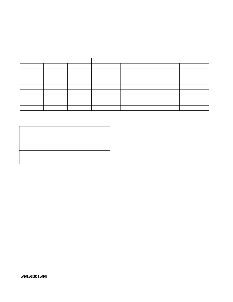
Table 1. Output Selection
Table 2. Mode Selection
1
1
1
1
0
0
1
1
0
0
0
1
0
1
0
1
ADDRESS
A1
0
1
OUT2
OUT3
OUT4
OUT5
OUT6
OUT7
OUT0
OUT1
OUT10
OUT11
OUT12
OUT13
OUT14
OUT15
OUT8
OUT9
OUT18
OUT19
OUT20
OUT21
OUT22
OUT23
OUT16
OUT17
OUTPUT SELECTED
MUX1
OUT26
OUT27
OUT28
OUT29
OUT30
OUT31
OUT24
OUT25
A2
A0
MUX0
MUX2
MUX3
0 = Logic Low, 1 = Logic High
0
1
Sample mode enabled on selected
analog multiplexer and channel
(Table 1).
Hold mode enabled on selected
analog multiplexer and channel
(Table 1).
MODE-SELECT
INPUTS* (M3–M0)
ACTION
0 = Logic Low, 1 = Logic High
*
Only one M_ input asserted low; all others must be logic high
to meet the timing specification (see Single vs. Simultaneous
Sampling).
相關(guān)PDF資料 |
PDF描述 |
|---|---|
| MAX5170AEEE | Low-Power, Serial, 14-Bit DACs with Voltage Output |
| MAX5170BEEE | Low-Power, Serial, 14-Bit DACs with Voltage Output |
| MAX5172AEEE | Low-Power, Serial, 14-Bit DACs with Voltage Output |
| MAX5172BEEE | Low-Power, Serial, 14-Bit DACs with Voltage Output |
| MAX5170 | Low-Power, Serial, 14-Bit DACs with Voltage Output |
相關(guān)代理商/技術(shù)參數(shù) |
參數(shù)描述 |
|---|---|
| MAX5166NECM+ | 功能描述:采樣&保持放大器 32Ch Sample/Hold Amp RoHS:否 制造商:Texas Instruments 通道數(shù)量:2 捕獲時間:20 us 電源電壓-最大:18 V 最大工作溫度:+ 85 C 最小工作溫度:- 25 C 安裝風格: 封裝 / 箱體:SOIC-14 封裝:Tube |
| MAX5166NECM+T | 功能描述:采樣&保持放大器 32Ch Sample/Hold Amp RoHS:否 制造商:Texas Instruments 通道數(shù)量:2 捕獲時間:20 us 電源電壓-最大:18 V 最大工作溫度:+ 85 C 最小工作溫度:- 25 C 安裝風格: 封裝 / 箱體:SOIC-14 封裝:Tube |
| MAX5166NECM-T | 功能描述:采樣&保持放大器 RoHS:否 制造商:Texas Instruments 通道數(shù)量:2 捕獲時間:20 us 電源電壓-最大:18 V 最大工作溫度:+ 85 C 最小工作溫度:- 25 C 安裝風格: 封裝 / 箱體:SOIC-14 封裝:Tube |
| MAX5167 | 制造商:MAXIM 制造商全稱:Maxim Integrated Products 功能描述:32-Channel Sample/Hold Amplifier with Output Clamping Diodes |
| MAX5167LCCM | 功能描述:采樣&保持放大器 RoHS:否 制造商:Texas Instruments 通道數(shù)量:2 捕獲時間:20 us 電源電壓-最大:18 V 最大工作溫度:+ 85 C 最小工作溫度:- 25 C 安裝風格: 封裝 / 箱體:SOIC-14 封裝:Tube |
發(fā)布緊急采購,3分鐘左右您將得到回復(fù)。