- 您現(xiàn)在的位置:買賣IC網(wǎng) > PDF目錄383427 > MAX5075BAUA (MAXIM INTEGRATED PRODUCTS INC) Push-Pull FET Driver with Integrated Oscillator and Clock Output PDF資料下載
參數(shù)資料
| 型號: | MAX5075BAUA |
| 廠商: | MAXIM INTEGRATED PRODUCTS INC |
| 元件分類: | MOSFETs |
| 英文描述: | Push-Pull FET Driver with Integrated Oscillator and Clock Output |
| 中文描述: | 3 A HALF BRDG BASED MOSFET DRIVER, PDSO8 |
| 封裝: | MO-187, MSOP-8 |
| 文件頁數(shù): | 2/8頁 |
| 文件大?。?/td> | 234K |
| 代理商: | MAX5075BAUA |
M
Push-Pull FET Driver with Integrated Oscillator
and Clock Output
2
_______________________________________________________________________________________
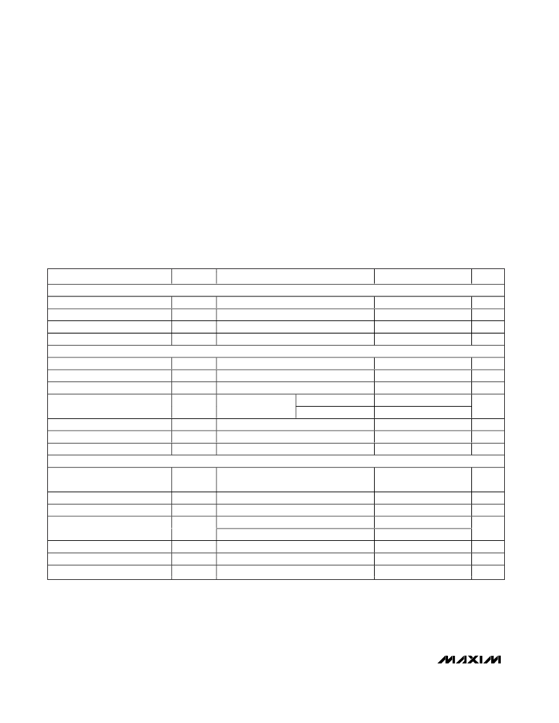
ABSOLUTE MAXIMUM RATINGS
V
CC
to DGND, PGND.............................................-0.3V to +18V
CLK, RT to DGND.....................................................-0.3V to +6V
NDRV1, NDRV2 to PGND...........................-0.3V to (V
CC
+ 0.3V)
DGND to PGND.....................................................-0.3V to +0.3V
CLK Current......................................................................±20mA
NDRV1, NDRV2 Peak Current (200ns)..................................±5A
NDRV1, NDRV2 Reverse Current (Latchup Current)......
±
500mA
ELECTRICAL CHARACTERISTICS
(V
CC
= +12V, R
RT
= 124k
, NDRV1 = NDRV2 = open, T
A
= T
J
= -40°C to +125°C, unless otherwise noted. Typical values are measured
at T
A
= +25
°
C.) (Note 1)
Stresses beyond those listed under “Absolute Maximum Ratings” may cause permanent damage to the device. These are stress ratings only, and functional
operation of the device at these or any other conditions beyond those indicated in the operational sections of the specifications is not implied. Exposure to
absolute maximum rating conditions for extended periods may affect device reliability.
Continuous Power Dissipation (T
A
= +70
°
C)
8-Pin μMAX (derate 10.3mW/
°
C above +70
°
C)...........825mW
Operating Temperature Range .........................-40
°
C to +125
°
C
Maximum Junction Temperature .....................................+150
°
C
Storage Temperature Range.............................-60
°
C to +150
°
C
Lead Temperature (soldering, 10s).................................+300
°
C
PARAMETER
SYMBOL
CONDITIONS
MIN
TYP
MAX
UNITS
SUPPLY
Input Voltage Supply Range
Switching Supply Current
Undervoltage Lockout
UVLO Hysteresis
OSCILLATOR
Frequency Range
Accuracy
Oscillator Jitter
V
CC
I
CCSW
V
UVLO
4.5
15.0
3
4
V
f
OSC
= 250kHz
V
CC
rising
1
mA
V
mV
3
3.5
300
f
OSC
(Note 2)
f
OSC
= 250kHz , 6V
≤
V
CC
≤
15V (Note 3)
50
-8
1500
+10
kHz
%
%
±0.6
7V
≤
V
CC
≤
15V
4.5V
≤
V
CC
≤
7V
4.1
3.5
5.0
5.0
50
CLK Output High Voltage
I
CLK
= 1mA
V
CLK Output Low Voltage
CLK Output Rise Time
CLK Output Fall Time
GATE DRIVERS (NDRV1, NDRV2)
I
CLK
= -1mA
C
CLK
= 30pF
C
CLK
= 30pF
mV
ns
ns
35
10
Output High Voltage
V
OH
I
NDRV1
= I
NDRV2
= 100mA
V
CC
-
0.3
V
Output Low Voltage
Output Peak Current
V
OL
I
P
I
NDRV1
= I
NDRV2
= -100mA
Sourcing and sinking
NDRV_ sourcing 100mA
NDRV_ sinking 100mA
Reverse current at NDRV1/NDRV2
C
LOAD
= 2nF
C
LOAD
= 2nF
0.3
V
A
3
1.8
1.6
400
10
10
3
Driver Output Impedance
2.6
Latchup Current Protection
Rise Time
Fall Time
mA
ns
ns
t
R
t
F
Note 1:
The MAX5075 is 100% tested at T
A
= T
J
= +125
°
C. All limits over temperature are guaranteed by design.
Note 2:
Use the following formula to calculate the MAX5075 oscillator frequency: f
OSC
= 10
12
/(32 x R
RT
).
Note 3:
The accuracy of the oscillator’s frequency is lower at frequencies greater than 1MHz.
相關PDF資料 |
PDF描述 |
|---|---|
| MAX5075C | Push-Pull FET Driver with Integrated Oscillator and Clock Output |
| MAX5075CAUA | Push-Pull FET Driver with Integrated Oscillator and Clock Output |
| MAX507AMRG | Voltage-Output, 12-Bit DACs with Internal Reference |
| MAX507-MAX508 | Voltage-Output, 12-Bit DACs with Internal Reference |
| MAX508BEWP | D/A CONVERTER |
相關代理商/技術參數(shù) |
參數(shù)描述 |
|---|---|
| MAX5075BAUA+ | 制造商:Maxim Integrated Products 功能描述:- Rail/Tube |
| MAX5075BAUA-T | 功能描述:功率驅動器IC Push-Pull FET Driver w/Osc & Clock RoHS:否 制造商:Micrel 產(chǎn)品:MOSFET Gate Drivers 類型:Low Cost High or Low Side MOSFET Driver 上升時間: 下降時間: 電源電壓-最大:30 V 電源電壓-最小:2.75 V 電源電流: 最大功率耗散: 最大工作溫度:+ 85 C 安裝風格:SMD/SMT 封裝 / 箱體:SOIC-8 封裝:Tube |
| MAX5075C | 制造商:MAXIM 制造商全稱:Maxim Integrated Products 功能描述:Push-Pull FET Driver with Integrated Oscillator and Clock Output |
| MAX5075CAUA | 功能描述:功率驅動器IC Push-Pull FET Driver w/Osc & Clock RoHS:否 制造商:Micrel 產(chǎn)品:MOSFET Gate Drivers 類型:Low Cost High or Low Side MOSFET Driver 上升時間: 下降時間: 電源電壓-最大:30 V 電源電壓-最小:2.75 V 電源電流: 最大功率耗散: 最大工作溫度:+ 85 C 安裝風格:SMD/SMT 封裝 / 箱體:SOIC-8 封裝:Tube |
| MAX5075CAUA+ | 制造商:Maxim Integrated Products 功能描述:- Rail/Tube |
發(fā)布緊急采購,3分鐘左右您將得到回復。