- 您現(xiàn)在的位置:買賣IC網(wǎng) > PDF目錄384681 > MAX503 (Maxim Integrated Products, Inc.) Low Power 5V RS232 Dual Driver/Receiver with 0.1?μF Capacitors; Package: SO; No of Pins: 16; Temperature Range: -40?°C to 85?°C PDF資料下載
參數(shù)資料
| 型號: | MAX503 |
| 廠商: | Maxim Integrated Products, Inc. |
| 元件分類: | 外設(shè)及接口 |
| 英文描述: | Low Power 5V RS232 Dual Driver/Receiver with 0.1?μF Capacitors; Package: SO; No of Pins: 16; Temperature Range: -40?°C to 85?°C |
| 中文描述: | 電可擦除可編程邏輯器件 |
| 文件頁數(shù): | 2/16頁 |
| 文件大小: | 118K |
| 代理商: | MAX503 |
M
5V, Low-Power, Parallel-Input,
Voltage-Output, 10-Bit DAC
2
_______________________________________________________________________________________
ABSOLUTE MAXIMUM RATINGS
V
DD
to DGND and V
DD
to AGND................................-0.3V, +6V
V
SS
to DGND and V
SS
to AGND .................................-6V, +0.3V
V
DD
to V
SS
............................................................... -0.3V, +12V
AGND to DGND........................................................-0.3V, +0.3V
REFGND to AGND.........................................-0.3V, (V
DD
+ 0.3V)
Digital Input Voltage to DGND .................... -0.3V, (V
DD
+ 0.3V)
REFIN..................................................(V
SS
- 0.3V), (V
DD
+ 0.3V)
REFOUT ..............................................(V
SS
- 0.3V), (V
DD
+ 0.3V)
REFOUT to REFGND.................................... -0.3V, (V
DD
+ 0.3V)
RFB ....................................................(V
SS
- 0.3V), (V
DD
+ 0.3V)
ROFS ..................................................(V
SS
- 0.3V), (V
DD
+ 0.3V)
VOUT to AGND (Note 1) .............................................. V
V
Continuous Current, Any Input ........................................±20mA
Continuous Power Dissipation (T
A
= +70°C)
Narrow Plastic DIP (derate 13.33mW/°C above +70°C)...1067mW
Wide SO (derate 11.76mW/°C above +70°C)............... 941mW
SSOP (derate 8.00mW/°C above +70°C) ......................640mW
Operating Temperature Ranges
MAX503C_G .........................................................0°C to +70°C
MAX503E_G ......................................................-40°C to +85°C
Storage Temperature Range.............................-65°C to +165°C
Lead Temperature (soldering, 10sec) ........................... +300°C
Stresses beyond those listed under “Absolute Maximum Ratings” may cause permanent damage to the device. These are stress ratings only, and functional
operation of the device at these or any other conditions beyond those indicated in the operational sections of the specifications is not implied. Exposure to
absolute maximum rating conditions for extended periods may affect device reliability.
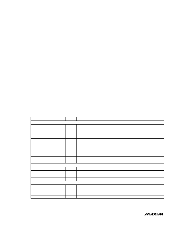
ELECTRICAL CHARACTERISTICS—Single +5V Supply
(V
DD
= 5V, V
SS
= 0V, AGND = DGND = REFGND = 0V, REFIN = 2.048V (external), RFB = ROFS = VOUT, C
REFOUT
= 33μF,
R
L
= 10k
, C
L
= 100pF, TA= TMINto TMAX, unless otherwise noted.)
PARAMETER
SYMBOL
MIN
TYP
MAX
UNITS
Differential Nonlinearity
Unipolar Offset Error
Unipolar Offset
Temperature Coefficient
Unipolar Offset-Error
Supply Rejection
DNL
V
OS
±1
3
LSB
LSB
0
0.25
TCV
OS
3
ppm/°C
PSRR
0.1
LSB/V
Resolution
Relative Accuracy
STATIC PERFORMANCE
N
10
Bits
LSB
Gain-Error Temperature Coefficient
Gain-Error Power-Supply Rejection
DAC VOLTAGE OUTPUT (VOUT)
Output Voltage Range
Resistive Load
DC Output Impedance
Short-Circuit Current
REFERENCE INPUT (REFIN)
Reference Input Range
Reference Input Resistance
Reference Input Capacitance
AC Feedthrough
1
ppm/°C
LSB/V
PSRR
0.1
0
2
V
DD
- 0.4
V
k
mA
0.2
12
I
SC
0
V
DD
- 2
V
40
10
k
pF
dB
50
-80
CONDITIONS
Guaranteed monotonic
4.5V
≤
V
DD
≤
5.5V
4.5V
≤
V
DD
≤
5.5V
VOUT = 2V, load regulation
≤
±0.5LSB
Code dependent, minimum at code 0101...
Code dependent (Note 3)
(Note 4)
Gain Error (Note 2)
GE
LSB
±1
Note 1:
The output may be shorted to V
, V
, DGND, or AGND if the continuous package power dissipation and current ratings
are not exceeded. Typical short-circuit currents are 20mA.
DAC latch = all 1s,
VOUT < V
DD
- 0.4V (Note 2)
INL
±0.5
(Note 2)
相關(guān)PDF資料 |
PDF描述 |
|---|---|
| MAX503EWG | 5V, Low-Power, Parallel-Input, Voltage-Output, 10-Bit DAC |
| MAX503CAG | Low Power 5V RS232 Dual Driver/Receiver with 0.1?μF Capacitors; Package: SO; No of Pins: 16; Temperature Range: -40?°C to 85?°C |
| MAX503CNG | Low Power 5V RS232 Dual Driver/Receiver with 0.1?μF Capacitors; Package: SO; No of Pins: 16; Temperature Range: -40?°C to 85?°C |
| MAX503CWG | Low Power 5V RS232 Dual Driver/Receiver with 0.1?μF Capacitors; Package: SO; No of Pins: 16; Temperature Range: -40?°C to 85?°C |
| MAX503EAG | Low Power 5V RS232 Dual Driver/Receiver with 0.1?μF Capacitors; Package: SO; No of Pins: 16; Temperature Range: -40?°C to 85?°C |
相關(guān)代理商/技術(shù)參數(shù) |
參數(shù)描述 |
|---|---|
| MAX-503-0512 | 制造商:SL Power Electronics 功能描述:AC/DC Power Supply Triple-OUT 5V/12V/-12V 80A/10A/10A 500W |
| MAX5033 | 制造商:MAXIM 制造商全稱:Maxim Integrated Products 功能描述:500mA, 76V, High-Efficiency, MAXPower Step-Down DC-DC Converter |
| MAX5033AAPA+ | 制造商:Maxim Integrated Products 功能描述:- Rail/Tube |
| MAX5033AASA | 功能描述:直流/直流開關(guān)轉(zhuǎn)換器 500mA 76V MAXPower Step-Down RoHS:否 制造商:STMicroelectronics 最大輸入電壓:4.5 V 開關(guān)頻率:1.5 MHz 輸出電壓:4.6 V 輸出電流:250 mA 輸出端數(shù)量:2 最大工作溫度:+ 85 C 安裝風(fēng)格:SMD/SMT |
| MAX5033AASA+ | 功能描述:直流/直流開關(guān)轉(zhuǎn)換器 500mA 76V MAXPower Step-Down RoHS:否 制造商:STMicroelectronics 最大輸入電壓:4.5 V 開關(guān)頻率:1.5 MHz 輸出電壓:4.6 V 輸出電流:250 mA 輸出端數(shù)量:2 最大工作溫度:+ 85 C 安裝風(fēng)格:SMD/SMT |
發(fā)布緊急采購,3分鐘左右您將得到回復(fù)。