- 您現(xiàn)在的位置:買(mǎi)賣(mài)IC網(wǎng) > PDF目錄11151 > MAX4647EUT-T (Maxim Integrated Products)IC SWITCH SPST SOT23-6 PDF資料下載
參數(shù)資料
| 型號(hào): | MAX4647EUT-T |
| 廠商: | Maxim Integrated Products |
| 文件頁(yè)數(shù): | 2/9頁(yè) |
| 文件大小: | 0K |
| 描述: | IC SWITCH SPST SOT23-6 |
| 產(chǎn)品培訓(xùn)模塊: | Lead (SnPb) Finish for COTS Obsolescence Mitigation Program |
| 標(biāo)準(zhǔn)包裝: | 2,500 |
| 功能: | 開(kāi)關(guān) |
| 電路: | 1 x SPST- NC |
| 導(dǎo)通狀態(tài)電阻: | 45 歐姆 |
| 電壓電源: | 單/雙電源 |
| 電壓 - 電源,單路/雙路(±): | 9 V ~ 36 V,±4.5 V ~ 20 V |
| 電流 - 電源: | 20µA |
| 工作溫度: | -40°C ~ 85°C |
| 安裝類(lèi)型: | 表面貼裝 |
| 封裝/外殼: | SOT-23-6 |
| 供應(yīng)商設(shè)備封裝: | SOT-6 |
| 包裝: | 帶卷 (TR) |
MAX4647/MAX4648
25 SPST Analog Switches in SOT23-6
2
_______________________________________________________________________________________
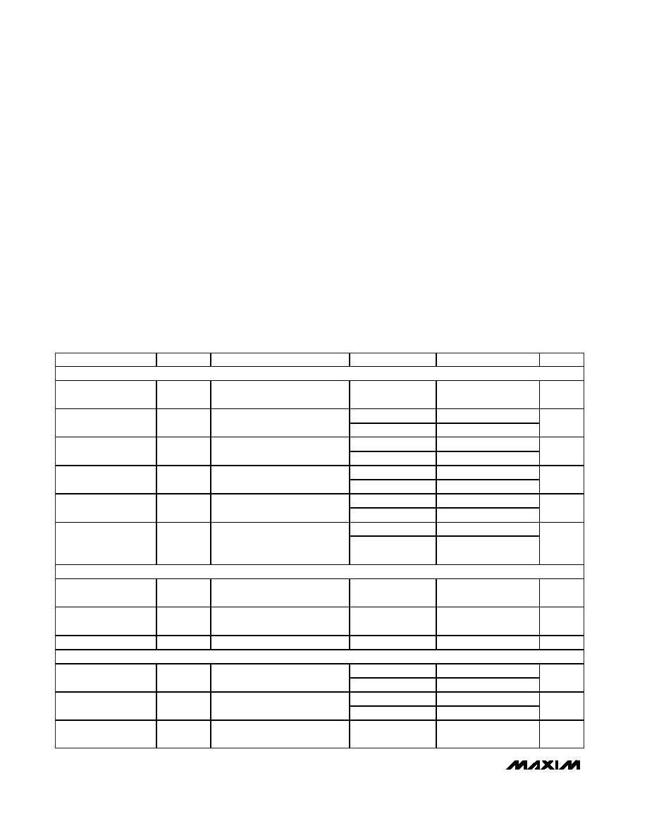
ABSOLUTE MAXIMUM RATINGS
ELECTRICAL CHARACTERISTICS—Dual ±15V Supplies
(V+ = +15V, V- = -15V, VIH = 2.4V, VIL = 0.8V, TA = TMIN to TMAX, unless otherwise noted. Typical values are at TA = +25°C.)
(Notes 2, 3)
Stresses beyond those listed under “Absolute Maximum Ratings” may cause permanent damage to the device. These are stress ratings only, and functional
operation of the device at these or any other conditions beyond those indicated in the operational sections of the specifications is not implied. Exposure to
absolute maximum rating conditions for extended periods may affect device reliability.
(Voltages referenced to GND)
V+ ...........................................................................-0.3V, +44.0V
V- ............................................................................-44.0V, +0.3V
V+ to V-................................................................-0.3V to +44.0V
All Other Pins (Note 1)...............................V- - 0.3V to V+ + 0.3V
Continuous Current into Any Terminal..............................±60mA
Peak Current into Any Terminal
(pulsed at 1ms, 10% duty cycle)...............................±100mA
Continuous Power Dissipation (TA = +70°C)
6-Pin SOT23 (derate 8.7mW/°C above +70°C)...........696mW
Operating Temperature Ranges
MAX464_EUT..................................................-40°C to +85°C
Storage Temperature Range .............................-65°C to +150°C
Junction Temperature ......................................................+150°C
Lead Temperature (soldering, 10s) .................................+300°C
PARAMETER
SYMBOL
CONDITIONS
TA
MIN
TYP
MAX
UNITS
ANALOG SWITCH
Analog Signal Range
VNO,VNC,
VCOM
V-
V+
V
+25
°C18
25
On-Resistance
RON
ICOM = 10mA; VNO
or VNC =
±10V
TMIN to TMAX
30
+25
°C
0.8
2
On-Resistance
Flatness (Note 4)
RFLAT(ON)
ICOM = 10mA; VNO
or VNC = +5V, 0, -5V
TMIN to TMAX
3
+25
°C-1
0.01
1
NO or NC Off-Leakage
Current
INO(OFF) or
INC(OFF)
VNO or VNC = +14V, -14V;
VCOM = -14V, +14V
TMIN to TMAX
-10
10
nA
+25
°C-1
0.01
1
COM Off-Leakage
Current
ICOM(OFF)
VCOM = -14V, +14V;
VNO or VNC = +14V, -14V
TMIN to TMAX
-10
10
nA
+25
°C-2
2
COM On-Leakage
Current
ICOM(ON)
VCOM = +14V, -14V;
VNO or VNC = +14V, -14V or
floating
TMIN to TMAX
-20
20
nA
LOGIC INPUT
Input Logic High
VIH
TMIN to TMAX
2.4
V
Input Logic Low
VIL
TMIN to TMAX
0.8
V
Input Leakage Current
IIN
VIN = 0 or +5V
TMIN to TMAX
-1
1
A
DYNAMIC CHARACTERISTICS
+25
°C68
100
Turn-On Time
tON
VNO or VNC =
±10V; RL = 300;
CL = 35pF; Figure 2
TMIN to TMAX
125
ns
+25
°C62
100
Turn-Off Time
tOFF
VNO or VNC =
±10V; RL =300;
CL = 35pF; Figure 2
TMIN to TMAX
125
ns
Charge Injection
Q
COM = 0; RS = 0; CL = 1nF;
Figure 3
+25
°C4
pC
Note 1: Signals on NO, NC, COM, or IN exceeding V+ or V- are clamped by internal diodes. Limit forward-diode current to
maximum current rating.
相關(guān)PDF資料 |
PDF描述 |
|---|---|
| VI-B1N-IY-F2 | CONVERTER MOD DC/DC 18.5V 50W |
| VI-21N-IY-F4 | CONVERTER MOD DC/DC 18.5V 50W |
| DG212CY+ | IC SWITCH QUAD SPST 16SOIC |
| VI-21N-IY-F3 | CONVERTER MOD DC/DC 18.5V 50W |
| DG211CY+ | IC SWITCH QUAD SPST 16SOIC |
相關(guān)代理商/技術(shù)參數(shù) |
參數(shù)描述 |
|---|---|
| MAX4648EUT | 制造商:Maxim Integrated Products 功能描述:25 OHM, SPST ANALOG SWITCHES IN SOT23-6. - Bulk |
| MAX4648EUT+ | 制造商:Maxim Integrated Products 功能描述:ANLG SW SGL SPST 20V/36V 6PIN SOT-23 - Rail/Tube |
| MAX4648EUT+T | 功能描述:模擬開(kāi)關(guān) IC 25Ohm SPST Analog Switch RoHS:否 制造商:Texas Instruments 開(kāi)關(guān)數(shù)量:2 開(kāi)關(guān)配置:SPDT 開(kāi)啟電阻(最大值):0.1 Ohms 切換電壓(最大): 開(kāi)啟時(shí)間(最大值): 關(guān)閉時(shí)間(最大值): 工作電源電壓:2.7 V to 4.5 V 最大工作溫度:+ 85 C 安裝風(fēng)格:SMD/SMT 封裝 / 箱體:DSBGA-16 |
| MAX4648EUT-T | 功能描述:模擬開(kāi)關(guān) IC 25Ohm SPST Analog Switch RoHS:否 制造商:Texas Instruments 開(kāi)關(guān)數(shù)量:2 開(kāi)關(guān)配置:SPDT 開(kāi)啟電阻(最大值):0.1 Ohms 切換電壓(最大): 開(kāi)啟時(shí)間(最大值): 關(guān)閉時(shí)間(最大值): 工作電源電壓:2.7 V to 4.5 V 最大工作溫度:+ 85 C 安裝風(fēng)格:SMD/SMT 封裝 / 箱體:DSBGA-16 |
| MAX4649EKA | 制造商:Maxim Integrated Products 功能描述:HIGH-VOLTAGE 45 OHM SPDT ANALOG S - Bulk |
發(fā)布緊急采購(gòu),3分鐘左右您將得到回復(fù)。