- 您現(xiàn)在的位置:買賣IC網(wǎng) > PDF目錄11564 > MAX3421EEHJ+T (Maxim Integrated Products)IC USB PERIPH/HOST CNTRL 32TQFP PDF資料下載
參數(shù)資料
| 型號: | MAX3421EEHJ+T |
| 廠商: | Maxim Integrated Products |
| 文件頁數(shù): | 9/28頁 |
| 文件大小: | 0K |
| 描述: | IC USB PERIPH/HOST CNTRL 32TQFP |
| 產(chǎn)品培訓(xùn)模塊: | Lead (SnPb) Finish for COTS Obsolescence Mitigation Program |
| 標(biāo)準(zhǔn)包裝: | 2,500 |
| 控制器類型: | USB 外設(shè)控制器 |
| 接口: | USB/串行 |
| 電源電壓: | 3 V ~ 3.6 V |
| 電流 - 電源: | 15mA |
| 工作溫度: | -40°C ~ 85°C |
| 安裝類型: | 表面貼裝 |
| 封裝/外殼: | 32-TQFP |
| 供應(yīng)商設(shè)備封裝: | 32-TQFP(5x5) |
| 包裝: | 帶卷 (TR) |
| 配用: | MAX3421EVKIT-1+-ND - EVAL KIT FOR MAX3421E |
第1頁第2頁第3頁第4頁第5頁第6頁第7頁第8頁當(dāng)前第9頁第10頁第11頁第12頁第13頁第14頁第15頁第16頁第17頁第18頁第19頁第20頁第21頁第22頁第23頁第24頁第25頁第26頁第27頁第28頁
MAX3421E
USB Peripheral/Host Controller
with SPI Interface
17
Maxim Integrated
RES
Drive
RES low to put the MAX3421E into a chip reset. A
chip reset sets all registers to their default states,
except for PINCTL (R17), USBCTL (R15), and SPI logic.
All FIFO contents are unknown during chip reset. Bring
the MAX3421E out of chip reset by driving
RES high.
The
RES pulse width can be as short as 200ns. See the
Device Reset section for a description of the resets
available on the MAX3421E.
INT
The MAX3421E INT output pin signals when a USB
event occurs that requires the attention of the SPI mas-
ter. INT can also be configured to assert when any of
the general-purpose inputs (GPIN0–GPIN7) are activat-
ed (see the
GPIN7–GPIN0 section for more details).
The SPI master must set the IE bit in the CPUCTL (R16)
register to activate INT. When the IE bit is cleared, INT
is inactive (open for level mode, high for negative edge,
low for positive edge). INT is inactive upon power-up or
after a chip reset (IE = 0).
The INT pin can be a push-pull or open-drain output.
Set the INTLEVEL bit of the PINCTL (R17) register high
to program the INT output pin to be an active-low level
open-drain output. An external pullup resistor to VL is
required for this setting. In level mode, the MAX3421E
drives INT low when any of the interrupt flags are set. If
multiple interrupts are pending, INT goes inactive only
when the SPI master clears the last active interrupt
request bit (Figure 12). The POSINT bit of the PINCTL
(R17) register has no effect on INT in level mode.
Clear the INTLEVEL bit to program INT to be an edge
active push-pull output. The active edge is programma-
ble using the POSINT bit of the PINCTL (R17) register.
In edge mode, the MAX3421E produces an edge refer-
enced to VL any time an interrupt request is activated,
or when an interrupt request is cleared and others are
pending (Figure 12). Set the POSINT bit in the PINCTL
(R17) register to make INT active high, and clear the
POSINT bit to make INT active low. The PULSEWID1
and PULSEWID0 bits in the CPUCTL (R16) register
control the pulse width of INT in edge mode as shown
in Table 4.
GPIN7–GPIN0
The SPI master samples GPIN3–GPIN0 states by read-
ing bit 7 through bit 4 of the IOPINS1 (R20) register.
GPIN7–GPIN4 states are sampled by reading bit 7
through bit 4 of the IOPINS2 (R21) register. Writing to
these bits has no effect.
Three registers, operational in both peripheral and host
mode, control eight interrupt requests from the
GPIN7–GPIN0 inputs. The GPINIRQ (R22) register con-
tains the interrupt request flags for the eight GPIN
inputs. The GPINIEN (R23) register contains individual
interrupt enable bits for the eight GPIN interrupts. The
GPINPOL (R24) register controls the edge polarity for
the eight GPIN interrupts. The eight GPIN interrupts are
added into the MAX3421E interrupt system and appear
on the INT output pin if enabled and asserted. It is also
possible to separate the GPIN interrupts and make them
available on the GPX output pin by setting SEPIRQ = 1.
This provides lower latency interrupt service since the
source of the interrupt on the GPX output is known, and
only the GPINIRQ register needs to be checked to
determine the interrupt source. Note that the GPINPOL
bits control the edge sensitivity of the GPIN transitions
as they set an internal “interrupt pending” flip-flop, not
the INT output pin. The INT pin output characteristics
are determined by the INTLEVEL and POSINT register
bits, as in the MAX3420E. If the GPX pin is configured
as the GPIN INT pin, its output characteristics are the
same as programmed for the INT pin.
Table 4. Pulse Width of INT Output
Configured by PULSEWID1 and
PULSEWID0
PULSEWID1
PULSEWID0
INT PULSE WIDTH (s)
0
10.6
0
1
5.3
1
0
2.6
1
1.3
CLEAR
FIRST IRQ,
SECOND
IRQ STILL
ACTIVE
SECOND
IRQ
ACTIVE
FIRST IRQ
ACTIVE
CLEAR
IRQ
SINGLE
IRQ
,
INTLEVEL = 1
POSINT = X
INTLEVEL = 0
POSINT = 0
INTLEVEL = 0
POSINT = 1
CLEAR
LAST
PENDING
IRQ
(1)
(2)
INT
(1) WIDTH DETERMINED BY TIME TAKEN TO CLEAR THE IRQ.
(2) WIDTH DETERMINED BY PULSEWID1 AND PULSEWID0 BITS IN CPUCTL (R16) REGISTER.
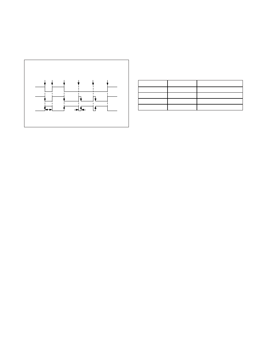
Figure 12. Behavior of the INT Pin for Different INTLEVEL and
POSINT Bit Settings
相關(guān)PDF資料 |
PDF描述 |
|---|---|
| GRM2165C1H510JZ01J | CAP CER 51PF 50V 5% NP0 0805 |
| MAX3421EETJ+T | IC USB PERIPH/HOST CNTRL 32TQFN |
| V375C28M75B3 | CONVERTER MOD DC/DC 28V 75W |
| MAX5942BESE+ | IC IEEE 802.3AF POE SYSTM 16SOIC |
| 78Q8430-100IGTR/F | IC LAN MEDIA ACCESS CTLR 100LQFP |
相關(guān)代理商/技術(shù)參數(shù) |
參數(shù)描述 |
|---|---|
| MAX3421EETJ+ | 功能描述:外圍驅(qū)動器與原件 - PCI USB Peripheral Controller w/SPI RoHS:否 制造商:PLX Technology 工作電源電壓: 最大工作溫度: 安裝風(fēng)格:SMD/SMT 封裝 / 箱體:FCBGA-1156 封裝:Tray |
| MAX3421EETJ+T | 功能描述:外圍驅(qū)動器與原件 - PCI USB Peripheral Controller w/SPI RoHS:否 制造商:PLX Technology 工作電源電壓: 最大工作溫度: 安裝風(fēng)格:SMD/SMT 封裝 / 箱體:FCBGA-1156 封裝:Tray |
| MAX3421EVKIT-1+ | 功能描述:界面開發(fā)工具 MAX3421E/20E Eval Kit RoHS:否 制造商:Bourns 產(chǎn)品:Evaluation Boards 類型:RS-485 工具用于評估:ADM3485E 接口類型:RS-485 工作電源電壓:3.3 V |
| MAX3430CPA | 功能描述:RS-485接口IC RoHS:否 制造商:Texas Instruments 數(shù)據(jù)速率:250 Kbps 工作電源電壓:3.3 V 電源電流:750 uA 工作溫度范圍:- 40 C to + 125 C 安裝風(fēng)格:SMD/SMT 封裝 / 箱體:SOIC-8 封裝:Tube |
| MAX3430CPA+ | 功能描述:RS-485接口IC Fail-Safe 1/4-Unit 3.3V Transceiver RoHS:否 制造商:Texas Instruments 數(shù)據(jù)速率:250 Kbps 工作電源電壓:3.3 V 電源電流:750 uA 工作溫度范圍:- 40 C to + 125 C 安裝風(fēng)格:SMD/SMT 封裝 / 箱體:SOIC-8 封裝:Tube |
發(fā)布緊急采購,3分鐘左右您將得到回復(fù)。