- 您現(xiàn)在的位置:買賣IC網(wǎng) > PDF目錄384656 > MAX2430IEE (MAXIM INTEGRATED PRODUCTS INC) Low-Voltage, Silicon RF Power Amplifier/Predriver PDF資料下載
參數(shù)資料
| 型號: | MAX2430IEE |
| 廠商: | MAXIM INTEGRATED PRODUCTS INC |
| 元件分類: | 衰減器 |
| 英文描述: | Low-Voltage, Silicon RF Power Amplifier/Predriver |
| 中文描述: | 800 MHz - 1000 MHz RF/MICROWAVE WIDE BAND MEDIUM POWER AMPLIFIER |
| 文件頁數(shù): | 5/10頁 |
| 文件大小: | 181K |
| 代理商: | MAX2430IEE |
M
Low-Voltage, S ilic on RF Power
Amplifier/Predriver
_______________________________________________________________________________________
5
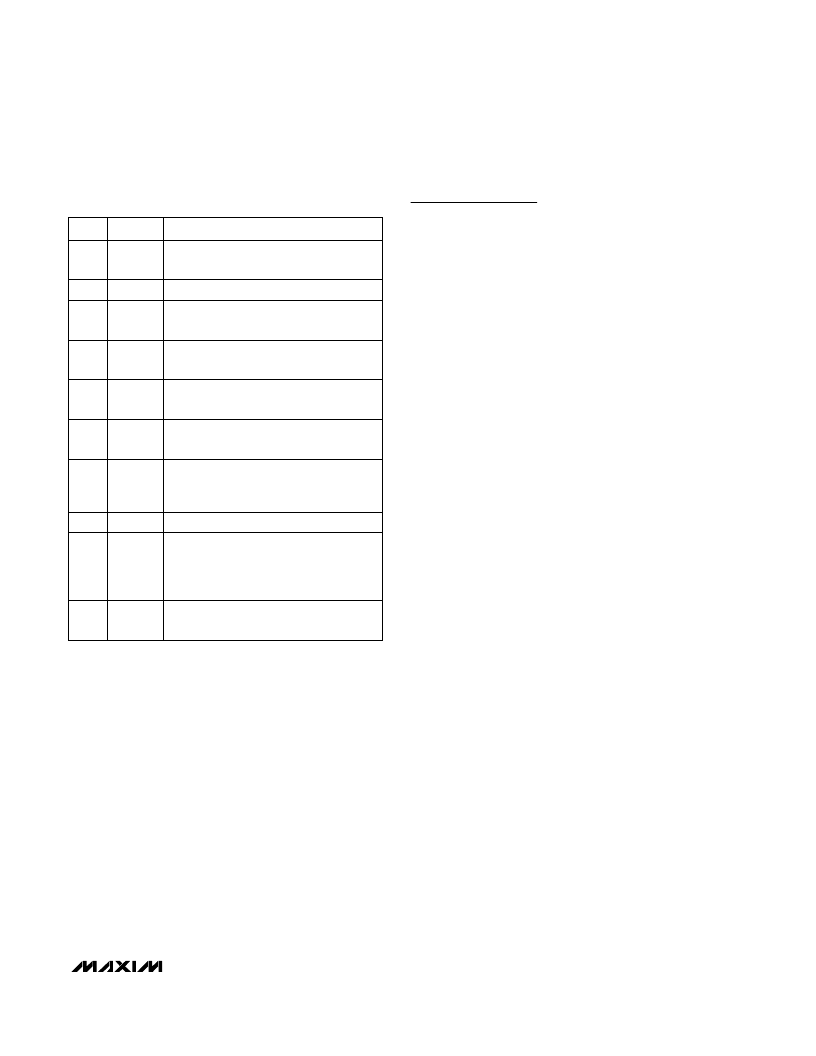
_____________________Pin Desc ription
NAME
FUNCTION
1, 15,
16
GND3
Driver Stage Ground. Connect directly to
ground plane.
2
SHDN
Shutdown Input (TTL/CMOS)
PIN
3, 5
GND2
Input Stage Ground. Connect directly to
ground plane.
4
RFIN
RF Input. Internally matched to 50
.
Requires series DC-blocking capacitor.
9
RFOUT
Output Transistor. Open Collector.
8
VCC2
Driver Stage Output. Connect to supply
through inductor (see Applications
Information.
7
VCC1
Bias Circuitry Supply. Connect to supply.
Bypass with 1000pF capacitor.
6
GND1
Bias Circuitry Ground. Connect directly to
ground plane.
11–14
GND4
Output Stage Ground. Connect directly to
ground plane.
10
BIAS
Output Stage Bias Pin. Connect capacitor
to GND to control start-up power enve-
lope. Drive directly for power control (see
Applications Information.
Detailed Desc ription
The MAX2430 consists of a large power output transis-
tor driven by a capacitively coupled driver stage (see
Functional Diagram. The driver and front-end gain
stages are DC-connected and biased on-chip from the
master bias cell. The master bias cell also controls the
output stage bias circuit. The input impedance at the
RFIN pin is internally matched to 50
, while the output
stage must be tuned and filtered externally for any nar-
row-band frequency range of interest between 800MHz
and 1000MHz.
The driver amplifier requires an external inductor at the
VCC2 pin to provide DC bias and proper matching to
the output stage. This inductor’s value depends on the
package type and frequency range of operation; typi-
cally it will vary between 5nH and 22nH.
The output transistor at the RFOUT pin requires an
external RF choke inductor connected to the supply for
DC bias, and a matching network to transform the
desired external load impedance to the optimal internal
load impedance of approximately 15
.
The MAX2430 includes a unique shutdown feature. The
TTL/CMOS-compatible
SHDN
input allows the device to
be shut down completely without the use of any exter-
nal components. Also, the RF output power envelope
ramp time can be programmed with a single external
capacitor connected between the BIAS pin and
ground. Pulling the shutdown pin (
SHDN
) high powers
on the master bias circuit, which in turn charges the
external capacitor tied to the BIAS pin using a con-
trolled current. The voltage at BIAS controls the output
power level, which ramps until the BIAS pin is internally
clamped to approximately 2.2V. The envelope ramp-
down time is controlled in a similar manner when the
SHDN
pin is pulled low.
Variable output power control over a 15dB range is also
possible by forcing the voltage on the BIAS pin exter-
nally from 0.6V to 2.4V.
During the on state (
SHDN
= high), the power-supply
bias current is typically 52mA with no RF applied to the
input. During the off state (
SHDN
= low), the supply
current is typically reduced to less than 1μA.
Note:
MAX2430IEE (PwrQSOP package) underside metal slug
must be soldered to PCB ground plane.
相關(guān)PDF資料 |
PDF描述 |
|---|---|
| MAX2430 | Low-Voltage, Silicon RF Power Amplifier/Predriver |
| MAX2450 | 3V, Ultra-Low-Power Quadrature Modulator/Demodulator |
| MAX2450CEP | 3V, Ultra-Low-Power Quadrature Modulator/Demodulator |
| MAX2451 | 3V, Ultra-Low-Power Quadrature Demodulator |
| MAX2451CSE | 3V, Ultra-Low-Power Quadrature Demodulator |
相關(guān)代理商/技術(shù)參數(shù) |
參數(shù)描述 |
|---|---|
| MAX2430ISE | 功能描述:RS-232接口集成電路 RoHS:否 制造商:Exar 數(shù)據(jù)速率:52 Mbps 工作電源電壓:5 V 電源電流:300 mA 工作溫度范圍:- 40 C to + 85 C 安裝風(fēng)格:SMD/SMT 封裝 / 箱體:LQFP-100 封裝: |
| MAX2430ISE-T | 功能描述:RS-232接口集成電路 RoHS:否 制造商:Exar 數(shù)據(jù)速率:52 Mbps 工作電源電壓:5 V 電源電流:300 mA 工作溫度范圍:- 40 C to + 85 C 安裝風(fēng)格:SMD/SMT 封裝 / 箱體:LQFP-100 封裝: |
| MAX2430PEVKIT | 功能描述:界面開發(fā)工具 RoHS:否 制造商:Bourns 產(chǎn)品:Evaluation Boards 類型:RS-485 工具用于評估:ADM3485E 接口類型:RS-485 工作電源電壓:3.3 V |
| MAX24310EVKIT# | 制造商:Microsemi Corporation 功能描述: 制造商:Microsemi Corporation 功能描述:MAX24310 EVALUATION KIT - Boxed Product (Development Kits) 制造商:Microsemi Corporation 功能描述:KIT EVALUATION MAX24310 |
| MAX24310EXG+ | 功能描述:時鐘發(fā)生器及支持產(chǎn)品 Not Available From Mouser RoHS:否 制造商:Silicon Labs 類型:Clock Generators 最大輸入頻率:14.318 MHz 最大輸出頻率:166 MHz 輸出端數(shù)量:16 占空比 - 最大:55 % 工作電源電壓:3.3 V 工作電源電流:1 mA 最大工作溫度:+ 85 C 安裝風(fēng)格:SMD/SMT 封裝 / 箱體:QFN-56 |
發(fā)布緊急采購,3分鐘左右您將得到回復(fù)。