- 您現(xiàn)在的位置:買賣IC網(wǎng) > PDF目錄385524 > MAX2386EBP-T (MAXIM INTEGRATED PRODUCTS INC) CDMA + GPS LNA/Mixers PDF資料下載
參數(shù)資料
| 型號: | MAX2386EBP-T |
| 廠商: | MAXIM INTEGRATED PRODUCTS INC |
| 元件分類: | 無繩電話/電話 |
| 英文描述: | CDMA + GPS LNA/Mixers |
| 中文描述: | TELECOM, CELLULAR, RF AND BASEBAND CIRCUIT, PBGA20 |
| 封裝: | 2.10 X 2.70 MM, UCSP-20 |
| 文件頁數(shù): | 10/18頁 |
| 文件大小: | 216K |
| 代理商: | MAX2386EBP-T |
M
receiving large signals, use LG mode to significantly
reduce current consumption (see the
R
BIAS
Switching
section).
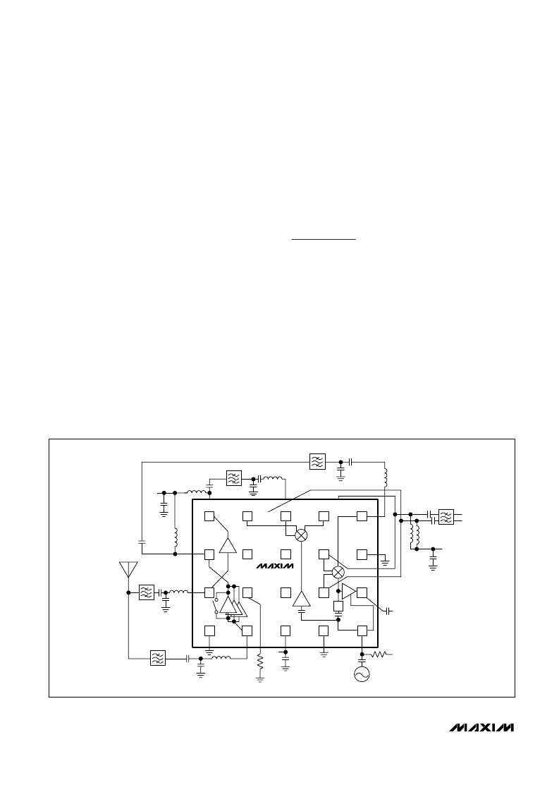
CDMA Downconverter
The CDMA mixer has four modes of operation for opti-
mal performance and current conservation. The logic
inputs MODE, G1, and G2 allow selection between the
different modes (Table 1).
The mixer output appears at the differential CIF+ and
CIF- pins. Each of these open-collector outputs
requires an external pullup inductor to V
CC
for DC bias-
ing. This port requires a matching network for coupling
to an external IF filter.
To further reduce board complexity, the CDMA and
GPS mixer outputs can be combined, eliminating one
of the IF filters (Figure 1).
LO Output Buffer
The LO_IN pin controls the LO output buffer. This pin
turns the open-collector LO output buffer on and off to
conserve current consumption as needed (see
Pin
Description
and
Typical Operating Circuits
).
RF Inputs
The mixer inputs CMIX_IN and GMIX_IN are typically
connected to the LNA output through an off-chip
image-reject bandpass filter. The LNA inputs and out-
puts require external matching networks to 50
.
Applications Information
R
BIAS
Switching
Figures 2 and 3 show more sophisticated methods of
varying the bias currents in different modes of opera-
tion. By adding a shunt resistor to R
BIAS
, the user can
increase or decrease the total bias resistance (and
therefore the bias current) in different modes, keeping
in mind that the voltage at the R
BIAS
pin is +1.2V.
Figure 2 uses a shunt resistor to decrease the total bias
resistance (when R
SHUNT
is tied low). This method
uses an additional DSP I/O control line. To avoid
adding an extra I/O line to the system, the user can use
the existing logic lines (MODE, G1, and G2). Figure 3
utilizes the G1 control pin, a transistor, and an addition-
al resistor to change the bias current in certain modes.
Both figures are simple ways to accommodate a wide
range of power schemes.
CDMA + GPS LNA/Mixers
Figure 1. Typical Operating Circuit with CDMA and GPS Mixers Combined
V
CC
D3
GND
VCO
BUFFEN
CLNAIN
D2
MODE
B3
CIF-
B4
G1
B2
GMXIN
A3
GIF+
A2
GLNAIN
GND
D1
RBIAS
C2
R
BIAS
GIF-
A4
CMXIN
A5
GND
B5
G2
CIF+
LO_OUT
C5
GLNAOUT
A1
V
CC
CLNAOUT
B1
C1
C3
C4
D4
D5
MAX2385
MAX2386
CDMA
GPS
GPS
/2
CDMA
V
CC
LO_IN
V
CC
CDMA IF
LO OUTPUT
10
______________________________________________________________________________________
相關(guān)PDF資料 |
PDF描述 |
|---|---|
| MAX2394 | MAX2394/MAX2395 Evaluation Kits |
| MAX2395 | MAX2394/MAX2395 Evaluation Kits |
| MAX2396 | Evaluation Kit |
| MAX2402EVKIT-SO | Evaluation Kit |
| MAX2402 | 800MHz to 1000MHz Transmitter(800MHz~1000MHz擴頻發(fā)送器) |
相關(guān)代理商/技術(shù)參數(shù) |
參數(shù)描述 |
|---|---|
| MAX2386EVKIT | 功能描述:射頻開發(fā)工具 RoHS:否 制造商:Taiyo Yuden 產(chǎn)品:Wireless Modules 類型:Wireless Audio 工具用于評估:WYSAAVDX7 頻率: 工作電源電壓:3.4 V to 5.5 V |
| MAX2387EGC | 功能描述:射頻混合器 RoHS:否 制造商:NXP Semiconductors 頻率范圍: 轉(zhuǎn)換損失——最大: 工作電源電壓:6 V 最大工作溫度:+ 85 C 最小工作溫度:- 40 C 安裝風格:Through Hole 封裝 / 箱體:PDIP-8 封裝:Tube |
| MAX2387EGC+ | 功能描述:射頻混合器 RoHS:否 制造商:NXP Semiconductors 頻率范圍: 轉(zhuǎn)換損失——最大: 工作電源電壓:6 V 最大工作溫度:+ 85 C 最小工作溫度:- 40 C 安裝風格:Through Hole 封裝 / 箱體:PDIP-8 封裝:Tube |
| MAX2387EGC-T | 功能描述:射頻混合器 RoHS:否 制造商:NXP Semiconductors 頻率范圍: 轉(zhuǎn)換損失——最大: 工作電源電壓:6 V 最大工作溫度:+ 85 C 最小工作溫度:- 40 C 安裝風格:Through Hole 封裝 / 箱體:PDIP-8 封裝:Tube |
| MAX2387ETC | 功能描述:射頻混合器 RoHS:否 制造商:NXP Semiconductors 頻率范圍: 轉(zhuǎn)換損失——最大: 工作電源電壓:6 V 最大工作溫度:+ 85 C 最小工作溫度:- 40 C 安裝風格:Through Hole 封裝 / 箱體:PDIP-8 封裝:Tube |
發(fā)布緊急采購,3分鐘左右您將得到回復(fù)。