- 您現(xiàn)在的位置:買賣IC網(wǎng) > PDF目錄385524 > MAX2370ETM (MAXIM INTEGRATED PRODUCTS INC) Complete 450MHz Quadrature Transmitter PDF資料下載
參數(shù)資料
| 型號: | MAX2370ETM |
| 廠商: | MAXIM INTEGRATED PRODUCTS INC |
| 元件分類: | 通信及網(wǎng)絡(luò) |
| 英文描述: | Complete 450MHz Quadrature Transmitter |
| 中文描述: | SPECIALTY TELECOM CIRCUIT, QCC48 |
| 封裝: | 7 X 7 MM, 0.80 MM HEIGHT, MO220, TQFN-48 |
| 文件頁數(shù): | 8/19頁 |
| 文件大小: | 387K |
| 代理商: | MAX2370ETM |
M
Detailed Description
The MAX2370 complete quadrature transmitter accepts
differential I/Q baseband inputs with external common-
mode bias. A modulator upconverts the baseband
inputs to a 95MHz to 195MHz IF frequency. A gain-con-
trol voltage pin (GC) controls the gain of both the IF and
RF VGAs simultaneously to achieve the best current
consumption and linearity performance. The IF signal is
brought off-chip for filtering, then fed to a single side-
band upconverter followed by the RF VGA and PA dri-
ver. The RF upconverter requires an external VCO for
operation. The IF PLL, RF PLL, and operating mode can
be programmed by an SPI/QSPI/ MICROWIRE-compati-
ble 3-wire interface.
The following sections describe each block in the
Functional Diagram
.
I/Q Modulator
Differential in-phase (I) and quadrature-phase (Q)
inputs are designed to be DC-coupled and biased with
the baseband output from a digital-to-analog converter
(DAC). The I and Q inputs need a typical DC bias of
V
CC
/ 2 and a current-drive capability of 8μA. However,
common-mode voltages in the 1.35V to (V
CC
- 1.25V)
range are also acceptable. The I and Q input capaci-
tances are typically 0.6pF to ground on each pin. The
IF VCO output is fed into a divide-by-two quadrature
generator block to derive quadrature LO components
to drive the I/Q modulator. The output of the modulator
is fed into the IF VGA.
IF VCO
The IF VCO oscillates at twice the desired IF frequency.
The oscillation frequency is determined by external tank
components (see the
IF Tank Design
section). Typical
spurious performance for the IF VCO is shown in the
Typical Operating Characteristics
.
IFLO Output Buffer
IFLO provides a buffered LO output when BUF_EN is 1.
The IFLO output frequency is equal to the IF VCO fre-
quency, and the typical output power is -12dBm. This
output is intended for applications where the receive IF
is the same frequency as the transmit IF.
IF/RF PLL
The IF/RF PLL uses a charge-pump output to drive exter-
nal loop filters. The loop filter is typically a passive sec-
ond-order lead-lag filter. Outside the filter
’
s bandwidth,
phase noise is determined by the tank components. The
two components that contribute most significantly to
phase noise are the inductor and varactor. Use high-Q
inductors and varactors to maximize equivalent parallel
resistance. The IF_TURBO_CHARGE, RCP_TURBO1,
and RCP_TURBO2 bits can be set to enable turbo mode.
Turbo mode provides maximum charge-pump current
during frequency acquisition. Turbo mode is disabled
after frequency acquisition is achieved. When turbo
mode is disabled, charge-pump current returns to the
programmed levels as set by the ICP and RCP bits in the
CONFIG register (Table 3).
IF VGA
The IF VGA allows the IF output level to be controlled by
a voltage applied to the GC pin. The 0.5V to 2.5V voltage
range on GC provides a gain-control range of > 70dB,
with 2.5V providing maximum gain. The differential IF
output ports are optimized for the 95MHz to 195MHz fre-
quency range. Do not allow V
GC
to exceed V
CC
- 0.2V
as this may cause oscillations at cold temperatures.
Single-Sideband Mixer and RF VGA
The RF transmit mixer uses a single-sideband architec-
ture to eliminate an off-chip RF filter. The RF VGA fol-
lows the single-sideband mixer and is controlled by the
same GC voltage as the IF VGA to provide optimum
Complete 450MHz Quadrature Transmitter
8
_______________________________________________________________________________________
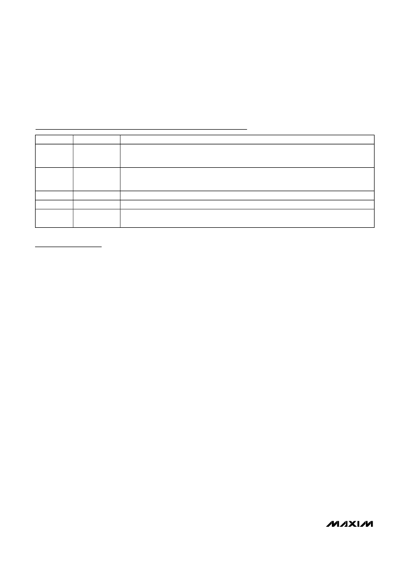
Pin Description (continued)
PIN
NAME
FUNCTION
40
RFCP
High-Impedance RF Charge-Pump Output. Connect to the tune input of the RF VCO through the
RF PLL loop filter. Keep the connection from RFCP to the tune input as short as possible to
prevent spurious pickup.
Power Supply for the RF Charge Pump. This supply can be different from the system V
CC
. Bypass
to PC board ground with a minimum 0.1μF capacitor placed as close to the pin as possible. Do
not share capacitor ground vias with other ground connections.
RF PLL Input. This port drives the RF PLL. RFPLL is internally biased to typically V
CC
- 0.8V.
RF LO Input. LO is internally biased to typically V
CC
- 0.8V.
Ground Connection. Solder the exposed paddle (EP) evenly to the board
’
s ground plane for
proper operation.
41
V
CCRFCP
42
44
RFPLL
LO
45, 46, 48,
EP
GND
相關(guān)PDF資料 |
PDF描述 |
|---|---|
| MAX2371EGC | LNAs with Step Attenuator and VGA |
| MAX2371ETC | LNAs with Step Attenuator and VGA |
| MAX2373EGC | LNAs with Step Attenuator and VGA |
| MAX2373ETC | LNAs with Step Attenuator and VGA |
| MAX2385EBP-T | CDMA + GPS LNA/Mixers |
相關(guān)代理商/技術(shù)參數(shù) |
參數(shù)描述 |
|---|---|
| MAX2370ETM+ | 功能描述:射頻發(fā)射器 Complete 450MHz Quadrature Txr RoHS:否 制造商:Micrel 類型:ASK Transmitter 封裝 / 箱體:SOT-23-6 工作頻率:300 MHz to 450 MHz 封裝:Reel |
| MAX2370ETM+T | 功能描述:射頻發(fā)射器 Complete 450MHz Quadrature Txr RoHS:否 制造商:Micrel 類型:ASK Transmitter 封裝 / 箱體:SOT-23-6 工作頻率:300 MHz to 450 MHz 封裝:Reel |
| MAX2370ETM-T | 功能描述:射頻發(fā)射器 Complete 450MHz Quadrature Txr RoHS:否 制造商:Micrel 類型:ASK Transmitter 封裝 / 箱體:SOT-23-6 工作頻率:300 MHz to 450 MHz 封裝:Reel |
| MAX2370EVKIT | 功能描述:射頻開發(fā)工具 MAX2370 Eval Kit RoHS:否 制造商:Taiyo Yuden 產(chǎn)品:Wireless Modules 類型:Wireless Audio 工具用于評估:WYSAAVDX7 頻率: 工作電源電壓:3.4 V to 5.5 V |
| MAX2371EGC | 功能描述:射頻放大器 RoHS:否 制造商:Skyworks Solutions, Inc. 類型:Low Noise Amplifier 工作頻率:2.3 GHz to 2.8 GHz P1dB:18.5 dBm 輸出截獲點:37.5 dBm 功率增益類型:32 dB 噪聲系數(shù):0.85 dB 工作電源電壓:5 V 電源電流:125 mA 測試頻率:2.6 GHz 最大工作溫度:+ 85 C 安裝風(fēng)格:SMD/SMT 封裝 / 箱體:QFN-16 封裝:Reel |
發(fā)布緊急采購,3分鐘左右您將得到回復(fù)。