- 您現(xiàn)在的位置:買賣IC網(wǎng) > PDF目錄10640 > MAX14780EESA+ (Maxim Integrated Products)IC TXRX RS485/422 ESD 8SO PDF資料下載
參數(shù)資料
| 型號(hào): | MAX14780EESA+ |
| 廠商: | Maxim Integrated Products |
| 文件頁數(shù): | 7/14頁 |
| 文件大?。?/td> | 0K |
| 描述: | IC TXRX RS485/422 ESD 8SO |
| 產(chǎn)品培訓(xùn)模塊: | Lead (SnPb) Finish for COTS Obsolescence Mitigation Program |
| 標(biāo)準(zhǔn)包裝: | 1 |
| 系列: | * |
2
Maxim Integrated
+5.0V, ±30kV ESD-Protected, Fail-Safe,
Hot-Swap, RS-485/RS-422 Transceiver
MAX14780E
Stresses beyond those listed under “Absolute Maximum Ratings” may cause permanent damage to the device. These are stress ratings only, and functional
operation of the device at these or any other conditions beyond those indicated in the operational sections of the specifications is not implied. Exposure to absolute
maximum rating conditions for extended periods may affect device reliability.
(All voltages referenced to GND.)
Supply Voltage (VCC)........................................................... +6V
Control Input Voltage (RE, DE) ...............................-0.3V to +6V
Driver Input Voltage (DI) .........................................-0.3V to +6V
Driver Output Voltage (A, B) ....................................-8V to +13V
Receiver Input Voltage (A, B) ..................................-8V to +13V
Receiver Output Voltage (RO) ................. -0.3V to (VCC + 0.3V)
Driver Output Current.................................................... ±250mA
Continuous Power Dissipation (TA = +70°C)
SO (derate 5.9mW/°C above +70°C) ..........................471mW
PDIP (derate 9.1mW/°C above +70°C) .....................727.3mW
Operating Temperature Range.......................... -40°C to +85°C
Junction Temperature .....................................................+150°C
Storage Temperature Range............................ -65°C to +150°C
Lead Temperature (soldering, 10s) ................................+300°C
Soldering Temperature (reflow) ......................................+260°C
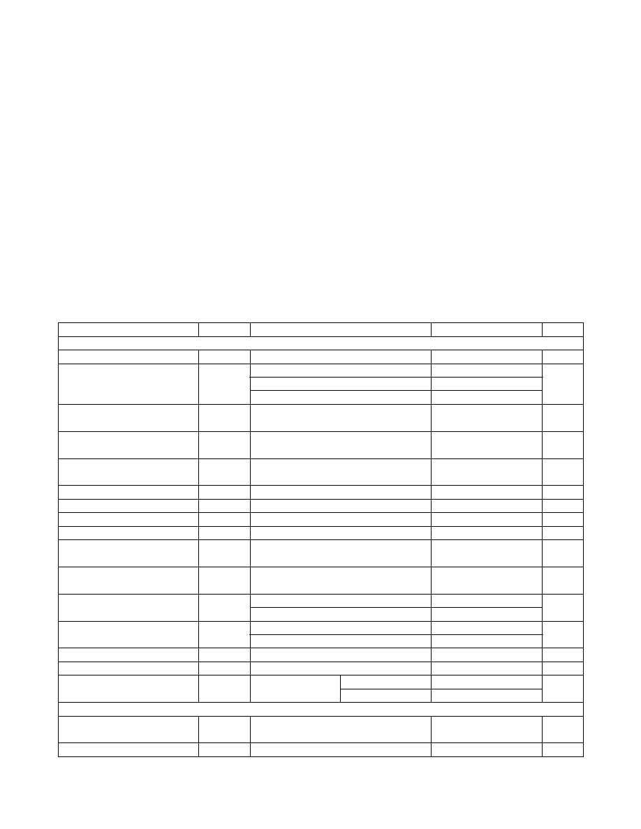
DC ELECTRICAL CHARACTERISTICS
(VCC = +5.0V ±10%, TA = TMIN to TMAX, unless otherwise noted. Typical values are at VCC = +5.0V and TA = +25NC.) (Note 1)
ABSOLUTE MAXIMUM RATINGS
PARAMETER
SYMBOL
CONDITIONS
MIN
TYP
MAX
UNITS
DRIVER
VCC Supply-Voltage Range
VCC
4.5
5.5
V
Differential Driver Output
VOD
RL = 100I (RS-422), Figure 1
3
VCC
V
RL = 54I (RS-485), Figure 1
2
VCC
No load
VCC
Change in Magnitude of
Differential Output Voltage
D
VOD
RL = 100I or 54I, Figure 1 (Note 2)
0.2
V
Driver Common-Mode Output
Voltage
VOC
RL = 100I or 54I, Figure 1
VCC/2
3
V
Change in Magnitude of
Common-Mode Voltage
D
VOC
RL = 100I or 54I, Figure 1 (Note 2)
0.2
V
Input-High Voltage
VIH
DE, DI, RE
3
V
Input-Low Voltage
VIL
DE, DI, RE
0.8
V
Input Hysteresis
VHYS
DE, DI, RE
100
mV
Input Current
IIN1
DE, DI, RE
Q
1
F
A
Input Impedance First Transition
at Power-Up
RPWUP
DE, RE = RE = 2V
3.65
8.8
kI
Input Impedance on First
Transition after POR Delay
Rft
DE = RE = 2V
7
60
k
Driver Short-Circuit Output
Current
IOSD
0 P VOUT P +12V (Note 3)
40
250
mA
-7V P VOUT P VCC (Note 3)
-250
-40
Driver Short-Circuit Foldback
Output Current
IOSDF
(VCC - 1V) P VOUT P +12V (Note 3)
20
mA
-7V P VOUT P +1V (Note 3)
-20
Thermal-Shutdown Threshold
TTS
175
N
C
Thermal-Shutdown Hysteresis
TTSH
15
N
C
Input Current (A and B)
IA, B
VDE = 0V,
VCC = 0V or VCC
VIN = +12V
125
F
A
VIN = -7V
-100
RECEIVER
Receiver Differential Threshold
Voltage
VTH
-7V P VCM P +12V
-200
-125
-50
mV
Receiver Input Hysteresis
D
VTH
VA + VB = 0V
15
mV
相關(guān)PDF資料 |
PDF描述 |
|---|---|
| HR10-10J-12S | JACK W/SOCKET INSERT (12 CON) |
| RM-15TRD-10S | RECEPTACLE W/SOCKET INSERT-10CON |
| MAX3469CSA+ | IC TXRX RS485/422 8-SOIC |
| MAX490ECSA+ | IC TXRX RS485/RS422 8-SOIC |
| RM-15TJD-10P | JACK EXT. W/PIN INSERT (10 CON) |
相關(guān)代理商/技術(shù)參數(shù) |
參數(shù)描述 |
|---|---|
| MAX14780EESA+ | 功能描述:RS-422/RS-485 接口 IC PROFIBUS RS-485 Transceiver RoHS:否 制造商:Maxim Integrated 數(shù)據(jù)速率:1136 Kbps 工作電源電壓:3 V to 5.5 V 電源電流:5.9 mA 工作溫度范圍:- 40 C to + 85 C 安裝風(fēng)格:SMD/SMT 封裝 / 箱體:SOIC-28 封裝:Tube |
| MAX14780EESA+T | 功能描述:RS-422/RS-485 接口 IC PROFIBUS RS-485 Transceiver RoHS:否 制造商:Maxim Integrated 數(shù)據(jù)速率:1136 Kbps 工作電源電壓:3 V to 5.5 V 電源電流:5.9 mA 工作溫度范圍:- 40 C to + 85 C 安裝風(fēng)格:SMD/SMT 封裝 / 箱體:SOIC-28 封裝:Tube |
| MAX14783EASA+ | 制造商:Maxim Integrated Products 功能描述:HALF DUPLEX, DUAL VOLTAGE (3V TO 5.5V), HIGH ESD HBM (+/-35K - Rail/Tube 制造商:Maxim Integrated Products 功能描述:IC TXRX RS485/422 ESD 8SO |
| MAX14783EASA+T | 制造商:Maxim Integrated Products 功能描述:HALF DUPLEX, DUAL VOLTAGE (3V TO 5.5V), HIGH ESD HBM (+/-35K - Tape and Reel 制造商:Maxim Integrated Products 功能描述:IC TXRX RS485/422 ESD 8SO |
| MAX14783EATA+ | 制造商:Maxim Integrated Products 功能描述:- Rail/Tube |
發(fā)布緊急采購,3分鐘左右您將得到回復(fù)。