- 您現(xiàn)在的位置:買賣IC網(wǎng) > PDF目錄224186 > MAX1396MTB+T (MAXIM INTEGRATED PRODUCTS INC) 1.5V to 3.6V, 312.5ksps, 1-Channel True-Differential/2-Channel Single-Ended, 12-Bit, SAR ADCs PDF資料下載
參數(shù)資料
| 型號(hào): | MAX1396MTB+T |
| 廠商: | MAXIM INTEGRATED PRODUCTS INC |
| 元件分類: | ADC |
| 英文描述: | 1.5V to 3.6V, 312.5ksps, 1-Channel True-Differential/2-Channel Single-Ended, 12-Bit, SAR ADCs |
| 中文描述: | 2-CH 12-BIT SUCCESSIVE APPROXIMATION ADC, SERIAL ACCESS, DSO10 |
| 封裝: | 3 X 3 MM, 0.80 MM HEIGHT, MO-229WEED-3, TDFN-10 |
| 文件頁(yè)數(shù): | 17/18頁(yè) |
| 文件大小: | 696K |
| 代理商: | MAX1396MTB+T |
第1頁(yè)第2頁(yè)第3頁(yè)第4頁(yè)第5頁(yè)第6頁(yè)第7頁(yè)第8頁(yè)第9頁(yè)第10頁(yè)第11頁(yè)第12頁(yè)第13頁(yè)第14頁(yè)第15頁(yè)第16頁(yè)當(dāng)前第17頁(yè)第18頁(yè)
MAX1393/MAX1396
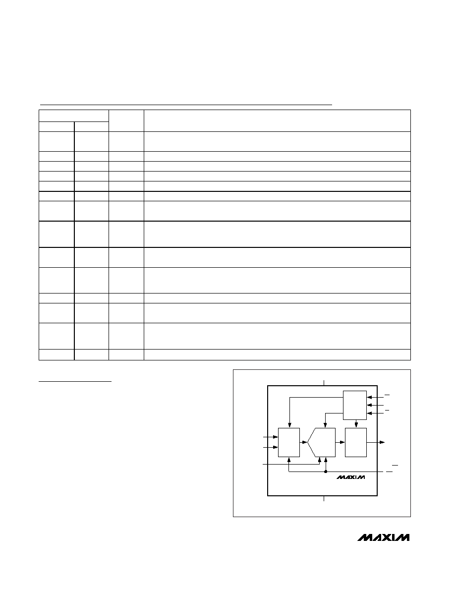
Detailed Description
The MAX1393/MAX1396 use an input track and hold
(T/H) circuit along with a SAR to convert an analog input
signal to a serial 12-bit digital output data stream. The
serial interface provides easy interfacing to microproces-
sors and DSPs. Figure 3 shows the simplified functional
diagram for the MAX1393 (1 channel, true differential)
and the MAX1396 (2 channels, single ended).
True-Differential Analog Input T/H
The equivalent input circuit of Figure 4 shows the
MAX1393/MAX1396 input architecture, which is com-
posed of a T/H, a comparator, and a switched-capacitor
DAC. The T/H enters its tracking mode on the falling
edge of CS (while OE is held low). The positive input
capacitor is connected to AIN+ (MAX1393), or to AIN1 or
AIN2 (MAX1396). The negative input capacitor is con-
nected to AIN- (MAX1393) or GND (MAX1396). The T/H
enters its hold mode on the 3rd falling edge of SCLK
8
_______________________________________________________________________________________
1.5V to 3.6V, 312.5ksps, 1-Channel True-Differential/
2-Channel Single-Ended, 12-Bit, SAR ADCs
PIN
MAX1393
MAX1396
NAME
FUNCTION
11
VDD
Positive Supply Voltage. Connect VDD to a 1.5V to 3.6V power supply. Bypass VDD to GND
with a 0.1F capacitor as close to the device as possible.
2
—
AIN-
Negative Analog Input
—
2
AIN2
Analog Input Channel 2
3
—
AIN+
Positive Analog Input
—
3
AIN1
Analog Input Channel 1
4
GND
Ground
5
REF
External Reference Voltage Input. VREF = 0.6V to (VDD + 0.05V). Bypass REF to GND with a
0.1F capacitor as close to the device as possible.
6
—
UNI/
BIP
Input-Mode Select. Drive UNI/
BIP high to select unipolar input mode. Pull UNI/BIP low to
select bipolar input mode. In unipolar mode, the output data is in straight binary format. In
bipolar mode, the output data is in two’s complement format.
—
6
CH1/CH2
Channel-Select Input. Pull
CH1/CH2 low to select channel 1. Drive CH1/CH2 high to select
channel 2.
77
OE
Active-Low Output Enable. Pull
OE low to enable DOUT. Drive OE high to disable DOUT.
Connect to
CS to interface with SPI, QSPI, and MICROWIRE devices or set low to interface
with DSP devices.
88
CS
Active-Low Chip-Select Input. A falling edge on
CS initiates power-up and acquisition.
9
DOUT
Serial-Data Output. DOUT changes state on the falling edge of SCLK. DOUT is high
impedance when
OE is high.
10
SCLK
Serial-Clock Input. SCLK drives the conversion process and clocks data out. Acquisition ends
on the 3rd falling edge after the
CS falling edge. The LSB is clocked out on the SCLK 15th
falling edge and the device enters AutoShutdown mode (see Figures 8 , 9, and 10).
——
EP
Exposed Pad. Not internally connected. Connect the exposed pad to GND or leave floating.
Pin Description
DOUT
VDD
REF
12-BIT SAR
ADC
CS
SCLK
OE
GND
OUTPUT
SHIFT
REGISTER
CONTROL
LOGIC AND
TIMING
*INDICATES THE MAX1396
AIN+ (AIN1)*
AIN- (AIN2)*
INPUT
MUX
AND T/H
UNI/BIP
(CH1/CH2)*
MAX1393
MAX1396
Figure 3. Simplified Functional Diagram
相關(guān)PDF資料 |
PDF描述 |
|---|---|
| MAX1396MUB+T | 1.5V to 3.6V, 312.5ksps, 1-Channel True-Differential/2-Channel Single-Ended, 12-Bit, SAR ADCs |
| MAX1396MUB+ | 1.5V to 3.6V, 312.5ksps, 1-Channel True-Differential/2-Channel Single-Ended, 12-Bit, SAR ADCs |
| MAX1416AEWE+ | 16-Bit, Low-Power, 2-Channel, Sigma-Delta ADCs |
| MAX1457AWI+T | 0.1% Accurate Signal Conditioner for Piezoresistive Sensor Compensation |
| MAX1457AWI+ | 0.1% Accurate Signal Conditioner for Piezoresistive Sensor Compensation |
相關(guān)代理商/技術(shù)參數(shù) |
參數(shù)描述 |
|---|---|
| MAX1396MUB | 功能描述:模數(shù)轉(zhuǎn)換器 - ADC RoHS:否 制造商:Texas Instruments 通道數(shù)量:2 結(jié)構(gòu):Sigma-Delta 轉(zhuǎn)換速率:125 SPs to 8 KSPs 分辨率:24 bit 輸入類型:Differential 信噪比:107 dB 接口類型:SPI 工作電源電壓:1.7 V to 3.6 V, 2.7 V to 5.25 V 最大工作溫度:+ 85 C 安裝風(fēng)格:SMD/SMT 封裝 / 箱體:VQFN-32 |
| MAX1396MUB+ | 功能描述:模數(shù)轉(zhuǎn)換器 - ADC 12-Bit 2Ch 312ksps 3.6V Precision ADC RoHS:否 制造商:Texas Instruments 通道數(shù)量:2 結(jié)構(gòu):Sigma-Delta 轉(zhuǎn)換速率:125 SPs to 8 KSPs 分辨率:24 bit 輸入類型:Differential 信噪比:107 dB 接口類型:SPI 工作電源電壓:1.7 V to 3.6 V, 2.7 V to 5.25 V 最大工作溫度:+ 85 C 安裝風(fēng)格:SMD/SMT 封裝 / 箱體:VQFN-32 |
| MAX1396MUB+T | 功能描述:模數(shù)轉(zhuǎn)換器 - ADC RoHS:否 制造商:Texas Instruments 通道數(shù)量:2 結(jié)構(gòu):Sigma-Delta 轉(zhuǎn)換速率:125 SPs to 8 KSPs 分辨率:24 bit 輸入類型:Differential 信噪比:107 dB 接口類型:SPI 工作電源電壓:1.7 V to 3.6 V, 2.7 V to 5.25 V 最大工作溫度:+ 85 C 安裝風(fēng)格:SMD/SMT 封裝 / 箱體:VQFN-32 |
| MAX1396MUB-T | 功能描述:模數(shù)轉(zhuǎn)換器 - ADC RoHS:否 制造商:Texas Instruments 通道數(shù)量:2 結(jié)構(gòu):Sigma-Delta 轉(zhuǎn)換速率:125 SPs to 8 KSPs 分辨率:24 bit 輸入類型:Differential 信噪比:107 dB 接口類型:SPI 工作電源電壓:1.7 V to 3.6 V, 2.7 V to 5.25 V 最大工作溫度:+ 85 C 安裝風(fēng)格:SMD/SMT 封裝 / 箱體:VQFN-32 |
| MAX139C/D | 功能描述:模數(shù)轉(zhuǎn)換器 - ADC RoHS:否 制造商:Texas Instruments 通道數(shù)量:2 結(jié)構(gòu):Sigma-Delta 轉(zhuǎn)換速率:125 SPs to 8 KSPs 分辨率:24 bit 輸入類型:Differential 信噪比:107 dB 接口類型:SPI 工作電源電壓:1.7 V to 3.6 V, 2.7 V to 5.25 V 最大工作溫度:+ 85 C 安裝風(fēng)格:SMD/SMT 封裝 / 箱體:VQFN-32 |
發(fā)布緊急采購(gòu),3分鐘左右您將得到回復(fù)。