- 您現(xiàn)在的位置:買賣IC網(wǎng) > PDF目錄383310 > MAX1127EGK (MAXIM INTEGRATED PRODUCTS INC) Quad, 12-Bit, 65Msps, 1.8V ADC with Serial LVDS Outputs PDF資料下載
參數(shù)資料
| 型號(hào): | MAX1127EGK |
| 廠商: | MAXIM INTEGRATED PRODUCTS INC |
| 元件分類: | ADC |
| 英文描述: | Quad, 12-Bit, 65Msps, 1.8V ADC with Serial LVDS Outputs |
| 中文描述: | 4-CH 12-BIT PROPRIETARY METHOD ADC, PARALLEL ACCESS, QCC68 |
| 封裝: | 10 X 10 MM, 0.90 MM HEIGHT, MO-220, QFN-68 |
| 文件頁(yè)數(shù): | 20/25頁(yè) |
| 文件大小: | 1661K |
| 代理商: | MAX1127EGK |
第1頁(yè)第2頁(yè)第3頁(yè)第4頁(yè)第5頁(yè)第6頁(yè)第7頁(yè)第8頁(yè)第9頁(yè)第10頁(yè)第11頁(yè)第12頁(yè)第13頁(yè)第14頁(yè)第15頁(yè)第16頁(yè)第17頁(yè)第18頁(yè)第19頁(yè)當(dāng)前第20頁(yè)第21頁(yè)第22頁(yè)第23頁(yè)第24頁(yè)第25頁(yè)
M
Quad, 12-Bit, 65Msps, 1.8V ADC with
Serial LVDS Outputs
20
______________________________________________________________________________________
Frame Alignment Output (FRAMEP, FRAMEN)
The MAX1127 provides a differential frame alignment
signal that consists of FRAMEP and FRAMEN. As shown
in Figure 4, the rising edge of the frame alignment sig-
nal corresponds to the first bit (D0) of the 12-bit serial
data stream. The frequency of the frame alignment sig-
nal is identical to the frequency of the sample clock.
Serial Output Data (OUT_P, OUT_N)
The MAX1127 provides its conversion results through
individual differential outputs consisting of OUT_P and
OUT_N. The results are valid 6.5 input clock cycles
after the sample is taken. As shown in Figure 3, the out-
put data is clocked out on both edges of the output
clock, LSB (D0) first. Figure 5 provides the detailed ser-
ial output timing diagram.
Output Data Format (
T
/B), Transfer Functions
The MAX1127 output data format is either offset binary or
two’s complement, depending on the logic input
T
/B.
With
T
/B low, the output data format is two’s comple-
ment. With
T
/B high, the output data format is offset bina-
ry. The following equations, Table 2, Figure 6, and Figure
7 define the relationship between the digital output and
the analog input. For two’s complement (
T
/B = 0):
and for offset binary (
T
/B = 1):
where CODE
10
is the decimal equivalent of the digital
output code as shown in Table 2. FSR is the full-scale
range as shown in Figures 6 and 7.
Keep the capacitive load on the MAX1127 digital out-
puts as low as possible.
LVDS and SLVS Signals (SLVS/
LVDS
)
Drive SLVS/
LVDS
low for LVDS or drive SLVS/
LVDS
high for scalable low-voltage signaling (SLVS) levels at
the MAX1127 outputs (OUT_P, OUT_N, CLKOUT_P,
CLKOUT_N, FRAMEP_, and FRAMEN_). See the
Electrical Characteristics
table for LVDS and SLVS out-
put voltage levels.
LVDS Test Pattern (LVDSTEST)
Drive LVDSTEST high to enable the output test pattern
on all LVDS or SLVS output channels. The output test
pattern is 0000 1011 1101 MSB
→
LSB. As with the ana-
log conversion results, the test pattern data is output
LSB first. Drive LVDSTEST low for normal operation
(test pattern disabled).
V
V
FSR
CODE
IN P
_
IN N
_
=
× ×
2048
4096
10
V
V
FSR
CODE
4096
IN P
_
IN N
_
=
× ×
10
(V
CLKOUTP
-
V
CLKOUTN
)
(V
OUT_P
-
V
OUT_N
)
t
CH
t
CL
t
OD
t
OD
D0
D1
D2
D3
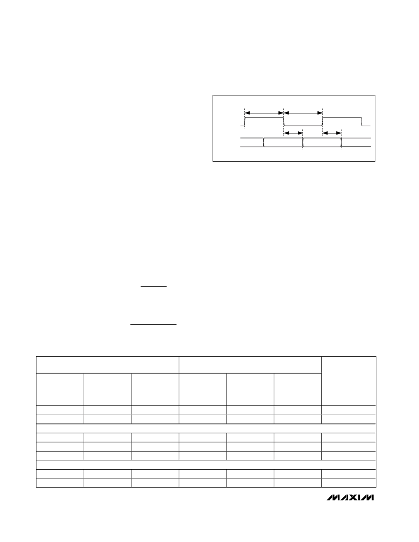
Figure 5. Serialized Output Detailed Timing Diagram
TWO’S COMPLEMENT DIGITAL OUTPUT CODE
(
T
/B = 0)
OFFSET BINARY DIGITAL OUTPUT CODE
(
T
/B = 1)
BINARY
D11
D0
HEXADECIMAL
EQUIVALENT
OF
D11
D0
DECIMAL
EQUIVALENT
OF
D11
D0
BINARY
D11
D0
HEXADECIMAL
EQUIVALENT
OF
D11
D0
DECIMAL
EQUIVALENT
OF
D11
D0
V
IN_P
- V
IN_P
(mV)
(V
REFIO
= 1.24V)
0111 1111 1111
0111 1111 1110
0x7FF
0x7FE
+2047
+2046
1111 1111 1111
1111 1111 1110
0xFFF
0xFFE
+4095
+4094
+699.66
+699.32
0000 0000 0001
0000 0000 0000
1111 1111 1111
0x001
0x000
0xFFF
+1
0
-1
1000 0000 0001
1000 0000 0000
0111 1111 1111
0x801
0x800
0x7FF
+2049
+2048
+2047
+0.34
0
-0.34
1000 0000 0001
1000 0000 0000
0X801
0x800
-2047
-2048
0000 0000 0001
0000 0000 0000
0x001
0x000
+1
0
-699.66
-700.00
Table 2. Output Code Table (V
REFIO
= 1.24V)
相關(guān)PDF資料 |
PDF描述 |
|---|---|
| MAX1134 | Low-Voltage Adjustable Precision Shunt Regulator 3-SOT-23 0 to 70 |
| MAX1134BCAP | Low-Voltage Adjustable Precision Shunt Regulator 3-SOT-23 0 to 70 |
| MAX1134BEAP | Low-Voltage Adjustable Precision Shunt Regulator 3-SOT-89 0 to 70 |
| MAX1135BCAP | Low-Voltage Adjustable Precision Shunt Regulator 3-SOT-89 0 to 70 |
| MAX1135BEAP | 16-Bit ADCs, 150ksps, 3.3V Single Supply |
相關(guān)代理商/技術(shù)參數(shù) |
參數(shù)描述 |
|---|---|
| MAX1127EGK+D | 制造商:Maxim Integrated Products 功能描述:ADC QUAD PIPELINED 65MSPS 12-BIT SERL 68QFN - Bulk |
| MAX1127EGK+TD | 制造商:Maxim Integrated Products 功能描述:ADC QUAD PIPELINED 65MSPS 12-BIT SERL 68QFN - Tape and Reel |
| MAX1127EVKIT | 制造商:Maxim Integrated Products 功能描述:QUAD 65MSPS 12-BIT ADC WITH SERIAL LVDS - Bulk |
| MAX113 | 制造商:MAXIM 制造商全稱:Maxim Integrated Products 功能描述:4-Digit.Up/Down Counter Decoder Driver[MM74C945/MM74C947/MM74C945C/D/MM74C945N ] |
| MAX1132 | 制造商:MAXIM 制造商全稱:Maxim Integrated Products 功能描述:16-Bit ADC, 200ksps, 5V Single-Supply with Reference |
發(fā)布緊急采購(gòu),3分鐘左右您將得到回復(fù)。