- 您現(xiàn)在的位置:買賣IC網(wǎng) > PDF目錄383308 > MAX1005EEE (MAXIM INTEGRATED PRODUCTS INC) IF Undersampler PDF資料下載
參數(shù)資料
| 型號: | MAX1005EEE |
| 廠商: | MAXIM INTEGRATED PRODUCTS INC |
| 元件分類: | 模擬信號調(diào)理 |
| 英文描述: | IF Undersampler |
| 中文描述: | SPECIALTY ANALOG CIRCUIT, PDSO16 |
| 封裝: | 0.150 INCH, 0.025 INCH PITCH, QSOP-16 |
| 文件頁數(shù): | 2/8頁 |
| 文件大小: | 95K |
| 代理商: | MAX1005EEE |
M
IF Undersampler
2
_______________________________________________________________________________________
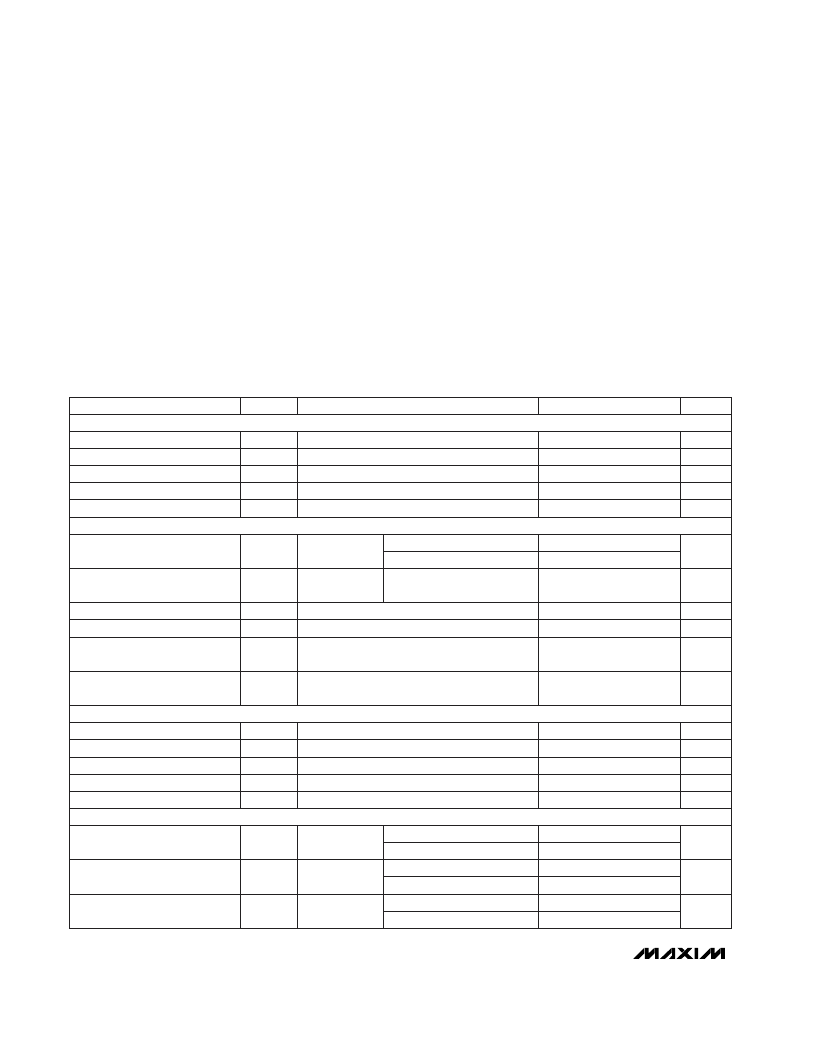
ABSOLUTE MAXIMUM RATINGS
VCCA to AGND ........................................................-0.3V, +6.0V
VCCD to DGND........................................................-0.3V, +6.0V
VCCA to VCCD ...................................................................±6.3V
Digital I/O Pins (D0–D6, CLK, RXEN, TXEN)
to DGND .................................-0.3V to (VCCD + 0.3V) or 6.0V
ELECTRICAL CHARACTERISTICS
(VCCA = VCCD = 3.0V, f
CLK
= 15MHz, R
L
=
∞
, T
A
= T
MIN
to T
MAX
, unless otherwise noted.)
SYMBOL
PARAMETER
TRANSMIT DAC DC ACCURACY
(Note 1)
Stresses beyond those listed under “Absolute Maximum Ratings” may cause permanent damage to the device. These are stress ratings only, and functional
operation of the device at these or any other conditions beyond those indicated in the operational sections of the specifications is not implied. Exposure to
absolute maximum rating conditions for extended periods may affect device reliability.
(whichever is smaller)
Analog I/O Pins (AIO+, AIO-)
to AGND................................(VCCA - 1.5V) to (VCCA + 0.3V)
AGND to DGND........................................................-0.3V, +0.3V
Power Dissipation (T
A
= +70°C)
QSOP (derate 5.90mW/°C above 70°C) ......................470mW
Operating Temperature Ranges
MAX1005CEE .....................................................0°C to +70°C
MAX1005EEE...................................................-40°C to +85°C
Storage Temperature Range.............................-65°C to +150°C
Lead Temperature (soldering, <10sec)...........................+300°C
(Notes 9, 10)
AIO+ = AIO-
(Note 4)
(Notes 6, 7)
(Note 3)
(Note 5)
CONDITIONS
-42
44
dB
-42
-24
THD
Total Harmonic Distortion
mV
368
400
432
V
IN
Full-Scale Input Range
RECEIVE ADC DYNAMIC PERFORMANCE
(T
A
= +25°C) (Note 8)
LSB
±2
Offset Error
LSB
±0.2
DNL
Differential Nonlinearity
LSB
±0.2
INL
Integral Nonlinearity
Bits
5
N
Resolution
dB
67
PSR
Power-Supply Rejection
CLK
period
0.5
DAC Latency
dBc
-50
Clock Feedthrough
μs
0.7
2.4
t
WAKE
Wakeup Time Exiting Shutdown
LSB
LSB
LSB
mVp-p
±0.2
±0.2
±1
±1
±1
864
INL
DNL
Integral Nonlinearity
Differential Nonlinearity
Offset Error
Transmit Full-Scale Output Voltage
TRANSMIT DAC DYNAMIC PERFORMANCE
(T
A
= +25°C) (Note 2)
Bits
7
N
Resolution
-28
dBc
THD+N
Total Harmonic Distortion plus
Noise
39
dBc
28
39
SFDR
Spurious-Free Dynamic Range
736
800
V
OUT
UNITS
MIN
TYP
MAX
VCCA = VCCD = 2.7V to 5.5V
VCCA = VCCD = 3.0V
VCCA = VCCD = 3.0V
VCCA = VCCD = 3.0V
VCC_ (A or D or both) = 3.0V ±100mVp-p at
100kHz
VCCA = VCCD = 2.7V to 5.5V
VCCA = VCCD = 3.0V
(Note 9)
(Note 9)
4.9
Bits
4.5
4.9
ENOB
Effective Number of Bits
44
dB
24
SFDR
Spurious-Free Dynamic Range
VCCA = VCCD = 2.7V to 5.5V
VCCA = VCCD = 3.0V
VCCA = VCCD = 2.7V to 5.5V
TRANSMIT ADC DC ACCURACY
(Note 8)
相關(guān)PDF資料 |
PDF描述 |
|---|---|
| MAX101 | 500Msps, 8-Bit ADC with Track/Hold |
| MAX101CFR | 500Msps, 8-Bit ADC with Track/Hold |
| MAX101A | 500Msps, 8-Bit ADC with Track/Hold |
| MAX1026ACEE-T | 10-Bit 300ksps ADCs with FIFO, Temp Sensor, Internal Reference |
| MAX1026AEEE-T | 10-Bit 300ksps ADCs with FIFO, Temp Sensor, Internal Reference |
相關(guān)代理商/技術(shù)參數(shù) |
參數(shù)描述 |
|---|---|
| MAX1005EEE+ | 功能描述:射頻無線雜項 IF Undersampler RoHS:否 制造商:Texas Instruments 工作頻率:112 kHz to 205 kHz 電源電壓-最大:3.6 V 電源電壓-最小:3 V 電源電流:8 mA 最大功率耗散: 工作溫度范圍:- 40 C to + 110 C 封裝 / 箱體:VQFN-48 封裝:Reel |
| MAX1005EEE+T | 功能描述:射頻無線雜項 IF Undersampler RoHS:否 制造商:Texas Instruments 工作頻率:112 kHz to 205 kHz 電源電壓-最大:3.6 V 電源電壓-最小:3 V 電源電流:8 mA 最大功率耗散: 工作溫度范圍:- 40 C to + 110 C 封裝 / 箱體:VQFN-48 封裝:Reel |
| MAX1005EEE-T | 功能描述:射頻無線雜項 RoHS:否 制造商:Texas Instruments 工作頻率:112 kHz to 205 kHz 電源電壓-最大:3.6 V 電源電壓-最小:3 V 電源電流:8 mA 最大功率耗散: 工作溫度范圍:- 40 C to + 110 C 封裝 / 箱體:VQFN-48 封裝:Reel |
| MAX1007 | 制造商:MAXIM 制造商全稱:Maxim Integrated Products 功能描述:Mobile-Radio Analog Controller |
| MAX1007CAG | 制造商:MAXIM 制造商全稱:Maxim Integrated Products 功能描述:Mobile-Radio Analog Controller |
發(fā)布緊急采購,3分鐘左右您將得到回復(fù)。