- 您現(xiàn)在的位置:買賣IC網(wǎng) > PDF目錄384643 > M66290AFP (Mitsubishi Electric Corporation) USB DEVICE CONTROLLER PDF資料下載
參數(shù)資料
| 型號(hào): | M66290AFP |
| 廠商: | Mitsubishi Electric Corporation |
| 英文描述: | USB DEVICE CONTROLLER |
| 中文描述: | USB設(shè)備控制器 |
| 文件頁數(shù): | 35/53頁 |
| 文件大?。?/td> | 435K |
| 代理商: | M66290AFP |
第1頁第2頁第3頁第4頁第5頁第6頁第7頁第8頁第9頁第10頁第11頁第12頁第13頁第14頁第15頁第16頁第17頁第18頁第19頁第20頁第21頁第22頁第23頁第24頁第25頁第26頁第27頁第28頁第29頁第30頁第31頁第32頁第33頁第34頁當(dāng)前第35頁第36頁第37頁第38頁第39頁第40頁第41頁第42頁第43頁第44頁第45頁第46頁第47頁第48頁第49頁第50頁第51頁第52頁第53頁
USB DEVICE CONTROLLER
M66290AGP/FP
MITSUBISHI <DIGITAL ASSP>
35
-
-
xxxx
W/R
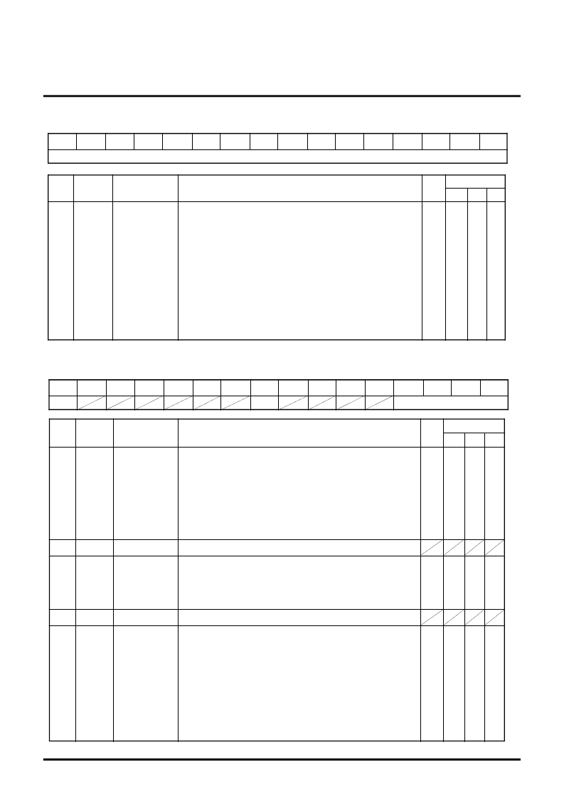
If the selected endpoint is set to OUT, this becomes to
receive data FIFO register.
If the selected endpoint is set to IN, this becomes to
transmit data FIFO register.
If the selected endpoint is set to 8-bit mode, lower 8 bit [7:0] is valid.
When read or write, 200ns (min) of cycle time is needed.
(Continuous access at 5MHz is available)
Read operation when direction IN is appointed or write operation
when direction OUT is appointed, write operation is inhibited.
CPU_FIFO data
CPU_FIFO
[15:0]
15 to 0
Bit
Bit
Name
Name
Function
W/R
USB
S/W
H/W
Reset
-
-
0
W/R
Set the operation mode of DMA transfer.
0 : High speed transfer mode
1 : One word transfer mode
In high speed transfer mode, when endpoint buffer is in read/write enable
in the state that DMA transfer enable, Dreq is asserted.
In one word transfer mode, when endpoint buffer is in read/write enable
in the state that DMA transfer enable and Dack="H", Dreq is asserted.
In both mode, Dreq detects Dack="L" and is negated.
DMA operation
mode
MODE
15
Reset
Function
Name
Bit
Name
Bit
Write/Read "0"
Reserved
14 to 9
-
-
0
W/R
-
-
0000
W/R
Write/Read "0"
Appoint the endpoint for DMA transfer.
"0001"=EP1,"0010"=EP2,"0011"=EP3,
"0100"=EP4,"0101"=EP5
EP0 can not be appointed.
Don't change the setting during write (IN) or read (OUT).
Change of the setting of the endpoint of direction IN must
be done after confirmed that IVAL="0" and Dreq="0", or
IVAL="1" and Dreq="1".
Change of the setting of the endpoint of direction OUT must
be done after confirmed that IVAL="0" and Dreq="1".
DMA transfer
endpoint
If this bit is "1", endpoint buffer which is appointed by DMA_EP[3:0]
is enable to write or when read is enable, Dreq is asserted.
If "0" is written in DMA transferring, DMA transfer is forced to end.
DMA transfer
enable
Reserved
DMA_EP
[3:0]
3 to 0
7 to 4
DMAEN
8
W/R
USB
S/W
H/W
MODE
DMAEN
DMA_EP[3:0]
D0
D1
D2
D3
D4
D5
D6
D7
D8
D9
D10
D11
D12
D15
D13
D14
(4-3) CPU_FIFO Data Register (Address : 44h)
(4-4) DMA_FIFO Selection Register (Address : 48h)
CPU_FIFO[15:0]
D0
D1
D2
D3
D4
D5
D6
D7
D8
D9
D10
D11
D12
D15
D13
D14
相關(guān)PDF資料 |
PDF描述 |
|---|---|
| M66290AGP | USB DEVICE CONTROLLER |
| M66300FP | PARALLEL-IN SERIAL-OUT DATA BUFFER WITH FIFO |
| M66300P | PARALLEL-IN SERIAL-OUT DATA BUFFER WITH FIFO |
| M66305AFP | TOGGLE LINE BUFFER |
| M66305AP | TOGGLE LINE BUFFER |
相關(guān)代理商/技術(shù)參數(shù) |
參數(shù)描述 |
|---|---|
| M66290AGP | 制造商:RENESAS 制造商全稱:Renesas Technology Corp 功能描述:USB DEVICE CONTROLLER |
| M66291GP | 制造商:Renesas Electronics Corporation 功能描述: |
| M66291GP#201 | 制造商:Renesas Electronics Corporation 功能描述:IC ASSP USB2.0 DEVICE CONTROLLER 48LQFP |
| M66291GP#RB0S | 功能描述:IC USB CONTROLLER GEN-PUR 48LQFP RoHS:是 類別:集成電路 (IC) >> 接口 - 控制器 系列:- 標(biāo)準(zhǔn)包裝:4,900 系列:- 控制器類型:USB 2.0 控制器 接口:串行 電源電壓:3 V ~ 3.6 V 電流 - 電源:135mA 工作溫度:0°C ~ 70°C 安裝類型:表面貼裝 封裝/外殼:36-VFQFN 裸露焊盤 供應(yīng)商設(shè)備封裝:36-QFN(6x6) 包裝:* 其它名稱:Q6396337A |
| M66291GPRB0S | 制造商:Renesas Electronics Corporation 功能描述:USB2.0 Device Controller,LQFP48 |
發(fā)布緊急采購,3分鐘左右您將得到回復(fù)。