- 您現(xiàn)在的位置:買賣IC網(wǎng) > PDF目錄370991 > M65617SP (Mitsubishi Electric Corporation) PICTURE-IN-PICTURE SIGNAL PROCESSING PDF資料下載
參數(shù)資料
| 型號: | M65617SP |
| 廠商: | Mitsubishi Electric Corporation |
| 英文描述: | PICTURE-IN-PICTURE SIGNAL PROCESSING |
| 中文描述: | 子母圖像信號處理 |
| 文件頁數(shù): | 1/15頁 |
| 文件大小: | 74K |
| 代理商: | M65617SP |

MITSUBISHI ICs (TV)
M65617SP
PICTURE-IN-PICTURE SIGNAL PROCESSING
1
DESCRIPTION
This system is an NTSC system PinP system that accommodates
subscreen composite input and main screen Y/C input. It is a
semiconductor IC circuit having a built-in 96K bit field memory and
an analog circuit, which permits a low-cost and compact system
configuration.
FEATURES
Built-in field memory 96K bit for PIP
Built-in luminance signal vertical filter
No. of subscreen displays: 1 (two sizes, 1/9 and 1/16, can be
selected from.)
No. of subscreen samples (1/9 - 1/16 sizes)
No. of quantization bits: 6 for all Y, B-Y and R-Y
No. of horizontal picture elements: 171(Y), 28.5 (B-Y, R-Y)
No. of vertical lines: 69/52
Subscreen frame display ON/OFF
Built-in analog circuits such as sync chip clamp, VCXO, and ana-
log switch
Built-in 2 channels of 8 bit A/D converter
(for main signal burst lock and PIP sub signal)
Built-in two channels of 8 bit D/A converter (luminance and
chroma signals)
I
C bus control
Controls: display ON/OFF, display size selection, setting of
display position, frame ON/OFF, setting of frame level, selection
of frame animation/field still image, setting of Y delay amount,
color level, tint, black level, etc.
2
APPLICATION
TV
RECOMMENDED OPERATING CONDITION
Supply voltage range........................................................3.1 to 3.5V
Operating frequency.........................................................14.32 MHz
Operating temperature....................................................-10 to 75
Input voltage (CMOS interface) "H"........................V
"L".............................0 to V
Output current (output buffer)........................................
°
C
V
DD
×
0.7 to V
DD
DD
×
0.3V
±
4mA (MAX)
Output load capacitance............................................20pF (MAX)
Circuit current.........................................................................140mA
1
NOTICE: Connect a 0.1
pins.
1 : Include pin capacitance (7pF)
μ
F or larger capacitor between V
DD
and V
SS
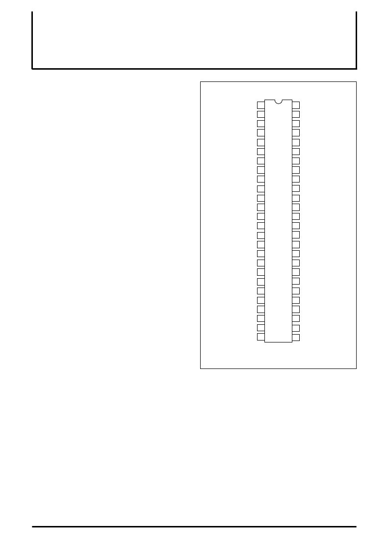
PIN CONFIGURATION (TOP VIEW)
AVss3 (vcxo)
VCXO out
VCXO in
FILTER
BIAS
AVdd3 (vcxo)
AVdd2 (m)
Vin (m)
Vrt (m)
Vrb (m)
AVss2 (m)
AVdd1 (s)
Vin (s)
Vrt (s)
AVssf (ana)
Cin
TESTEN
Yin
TEST9
C-PIP
TEST8
Y-PIP
AVdd4 (da)
C-PIPin
AVss4 (da)
Y-PIPin
ADJ-Ysub
Yout-sub
Outline 52P4B
52
49
50
51
1
4
3
2
48
5
47
6
44
9
43
10
42
11
41
12
13
14
40
39
7
8
46
45
15
38
16
37
17
36
18
35
19
20
34
33
21
32
22
31
23
24
30
29
25
28
26
27
Vrb (s)
AVss1 (s)
RESET
DVss1
DVdd1
BGP(s)/TEST0
SCK
CSYNC(s)/TEST1
ACK
DATA
CLK
DVss2
ADJ-Csub
Cout-sub
DVss3 (ram)
DVdd3 (ram)
SWMG/TEST7
SWM/TEST4
HD/TEST5
VD/CSYNC/TEST6
MCK
fsc/TEST3
BGP(m)/TEST2
DVdd2
M
相關(guān)PDF資料 |
PDF描述 |
|---|---|
| M65675FP | DIGITAL NTSC/PAL ENCODER |
| M65676FP | DIGITAL NTSC/PAL ENCODER |
| M65677FP | DIGITAL NTSC/PAL ENCODER |
| M65727FP | MPEG2 MOTION ESTIMATION LSI |
| M65824FP | SIGNAL PROCESSOR FOR CD PLAYER WITH BUILT-IN D/A |
相關(guān)代理商/技術(shù)參數(shù) |
參數(shù)描述 |
|---|---|
| M65656FP | 制造商:MITSUBISHI 制造商全稱:Mitsubishi Electric Semiconductor 功能描述:SCAN CONVERTER |
| M65657FP | 制造商:MITSUBISHI 制造商全稱:Mitsubishi Electric Semiconductor 功能描述:SCAN CONVERTER |
| M65664FP | 制造商:MITSUBISHI 制造商全稱:Mitsubishi Electric Semiconductor 功能描述:PICTURE-IN-PICTURE SIGNAL PROCESSING |
| M65665 | 制造商:MITSUBISHI 制造商全稱:Mitsubishi Electric Semiconductor 功能描述:PICTURE-IN-PICTURE SIGNAL PROCESSING |
| M65665CFP | 制造商:Panasonic Industrial Company 功能描述:IC |
發(fā)布緊急采購,3分鐘左右您將得到回復(fù)。