- 您現(xiàn)在的位置:買賣IC網(wǎng) > PDF目錄370991 > M64893AFP (Mitsubishi Electric Corporation) SERIAL INPUT PLL FREQUENCY SYNTHESIZER FOR TV/VCR PDF資料下載
參數(shù)資料
| 型號(hào): | M64893AFP |
| 廠商: | Mitsubishi Electric Corporation |
| 英文描述: | SERIAL INPUT PLL FREQUENCY SYNTHESIZER FOR TV/VCR |
| 中文描述: | 串行輸入鎖相環(huán)頻率合成器的電視/錄像機(jī) |
| 文件頁數(shù): | 3/7頁 |
| 文件大小: | 49K |
| 代理商: | M64893AFP |

MITSUBISHI IC
M64893FP/GP
S
(TV)
SERIAL INPUT PLL FREQUENCY SYNTHESIZER FOR TV/VCR
3
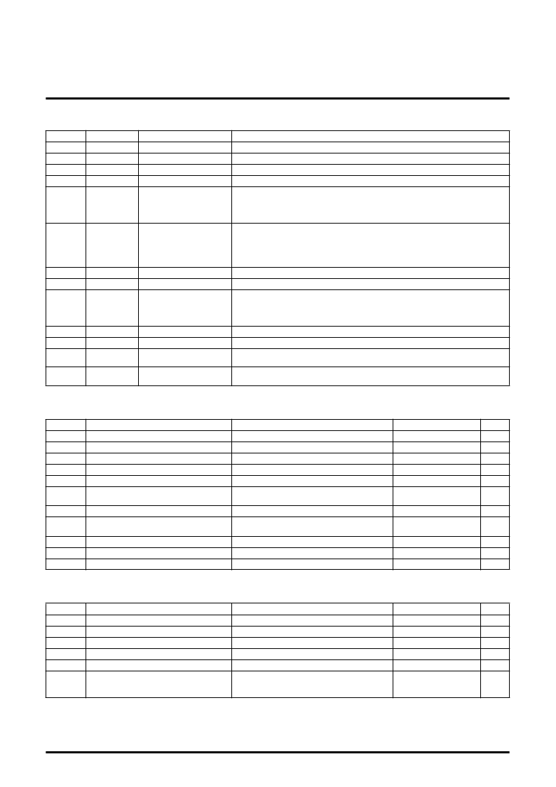
DESCRIPTION OF PIN
ABSOLUTE MAXIMUM RATINGS
(Ta=-20
°
C to +75
°
C, unless otherwise noted)
RECOMMENDED OPERATING CONDITIONS
(Ta=-20
°
C to +75
°
C, unless otherwise noted)
Pin No.
1
2
3
4
5
6
7
8
Symbol
Pin name
Function
fin
GND
V
CC1
V
CC2
BS4
BS3
BS2
BS1
Prescaler input
GND
Power supply voltage 1
Power supply voltage 2
Input for the VCO frequency.
Ground to 0V.
Power supply voltage terminal. 5.0V
Power supply for band switching, Vcc
±
0.5V
to 13.2V
1
Band switching outputs
PNP open collector method is used.
When the band switching data is "H", the output is ON.
When it is "L", the output is OFF.
9
Vin
Filter input
(Charge pump output)
This is the output terminal for the LPF input and charge pump output. When the
phase of the programmable divider output (f 1/N) is ahead compared to the
reference frequency (fref), the "source" current state becomes active.
If it is behind, the "sink" current becomes active.
If the phases are the same, the high impedance state becomes active.
This supplies the tuning voltage.
Power supply voltage for tuning voltage 28 to 35V
When 19 bit data is input,lock detector is output.
When 27 bit data is input, lock detector is output, the programmable freq.
Divider output and reference freq.
Output is selected by the test mode.
Data is read into the shift register when the clock signal falls.
Input for band SW and programmable freq. divider set up.
This is normally at a "L". When this is at "H", data and clock signals are received.
Data is read into the latch when the 19th pulse of the clock signal falls.
10
11
Vtu
V
CC3
Tuning output
Power supply voltage 3
12
LD/ftest
Lock detect/Test port
13
14
CLK
DATA
Clock input
Data input
15
ENA
Enable input
16
Xin
This is connected to the
crystal oscillator
4.0MHz crystal oscillator is connected.
Symbol
V
CC1
V
CC2
V
CC3
V
I
V
O
Parameter
Conditions
Ratings
6.0
14.4
36.0
6.0
6.0
Unit
V
V
V
V
V
Supply voltage 1
Supply voltage 2
Supply voltage 3
Input voltage
Output voltage
Voltage applied when the band output is
OFF
Band output current
Pin3
Pin4
Pin11
Not to exceed V
LD output
CC1
V
BSOFF
14.4
V
I
BSON
Per 1 band output circuit
50mA per 1 band output circuit
3circuit are pn at same time
Ta=+75
°
C
50.0
mA
t
BSON
ON the time when the band output is ON
10
sec
P
T
T
d
Power dissipation
Operating temperature
Storage temperature
470
mW
°
C
°
C
opr
-20 to +75
-40 to +125
stg
Symbol
V
CC1
V
CC2
V
CC3
f
opr1
f
opr2
Parameter
Conditions
Ratings
4.5 to 5.5
V
CC1
to 13.2
28 to 35
4.0
80 to 1,300
Unit
V
V
V
MHz
MHz
Supply voltage 1
Supply voltage 2
Supply voltage 3
Operating frequency (1)
Operating frequency (2)
Pin3
Pin4
Pin11
Crystal oscillation circuit
I
BDL
Band output current 5 to 8
Normally 1 circuit is on. 2 circuits on at the
same time is max. It is prohibited to have
3 or more circuits turned on at the same time.
0 to 40
mA
相關(guān)PDF資料 |
PDF描述 |
|---|---|
| M64893AGP | SERIAL INPUT PLL FREQUENCY SYNTHESIZER FOR TV/VCR |
| M64893FP | SERIAL INPUT PLL FREQUENCY SYNTHESIZER FOR TV/VCR |
| M64894 | SERIAL INPUT PLL FREQUENCY SYNTHESIZER FOR TV/VCR |
| M64894FP | SERIAL INPUT PLL FREQUENCY SYNTHESIZER FOR TV/VCR |
| M64894GP | SERIAL INPUT PLL FREQUENCY SYNTHESIZER FOR TV/VCR |
相關(guān)代理商/技術(shù)參數(shù) |
參數(shù)描述 |
|---|---|
| M64893AGP | 制造商:MITSUBISHI 制造商全稱:Mitsubishi Electric Semiconductor 功能描述:SERIAL INPUT PLL FREQUENCY SYNTHESIZER FOR TV/VCR |
| M64893FP | 制造商:MITSUBISHI 制造商全稱:Mitsubishi Electric Semiconductor 功能描述:SERIAL INPUT PLL FREQUENCY SYNTHESIZER FOR TV/VCR |
| M64893GP | 制造商:MITSUBISHI 制造商全稱:Mitsubishi Electric Semiconductor 功能描述:SERIAL INPUT PLL FREQUENCY SYNTHESIZER FOR TV/VCR |
| M64894 | 制造商:MITSUBISHI 制造商全稱:Mitsubishi Electric Semiconductor 功能描述:SERIAL INPUT PLL FREQUENCY SYNTHESIZER FOR TV/VCR |
| M64894FP | 制造商:MITSUBISHI 制造商全稱:Mitsubishi Electric Semiconductor 功能描述:SERIAL INPUT PLL FREQUENCY SYNTHESIZER FOR TV/VCR |
發(fā)布緊急采購,3分鐘左右您將得到回復(fù)。