- 您現(xiàn)在的位置:買賣IC網(wǎng) > PDF目錄377829 > M50FLW040BN5TP (意法半導(dǎo)體) 4 Mbit (5 x 64KByte Blocks + 3 x 16 x 4KByte Sectors) 3V Supply Firmware Hub / Low Pin Count Flash Memory PDF資料下載
參數(shù)資料
| 型號: | M50FLW040BN5TP |
| 廠商: | 意法半導(dǎo)體 |
| 英文描述: | 4 Mbit (5 x 64KByte Blocks + 3 x 16 x 4KByte Sectors) 3V Supply Firmware Hub / Low Pin Count Flash Memory |
| 中文描述: | 4兆位(5 × 64KB之座3 × 16 × 4KB的部門)3V電源固件集線器/低引腳數(shù)快閃記憶體 |
| 文件頁數(shù): | 12/52頁 |
| 文件大?。?/td> | 417K |
| 代理商: | M50FLW040BN5TP |
第1頁第2頁第3頁第4頁第5頁第6頁第7頁第8頁第9頁第10頁第11頁當(dāng)前第12頁第13頁第14頁第15頁第16頁第17頁第18頁第19頁第20頁第21頁第22頁第23頁第24頁第25頁第26頁第27頁第28頁第29頁第30頁第31頁第32頁第33頁第34頁第35頁第36頁第37頁第38頁第39頁第40頁第41頁第42頁第43頁第44頁第45頁第46頁第47頁第48頁第49頁第50頁第51頁第52頁
M50FLW040A, M50FLW040B
12/52
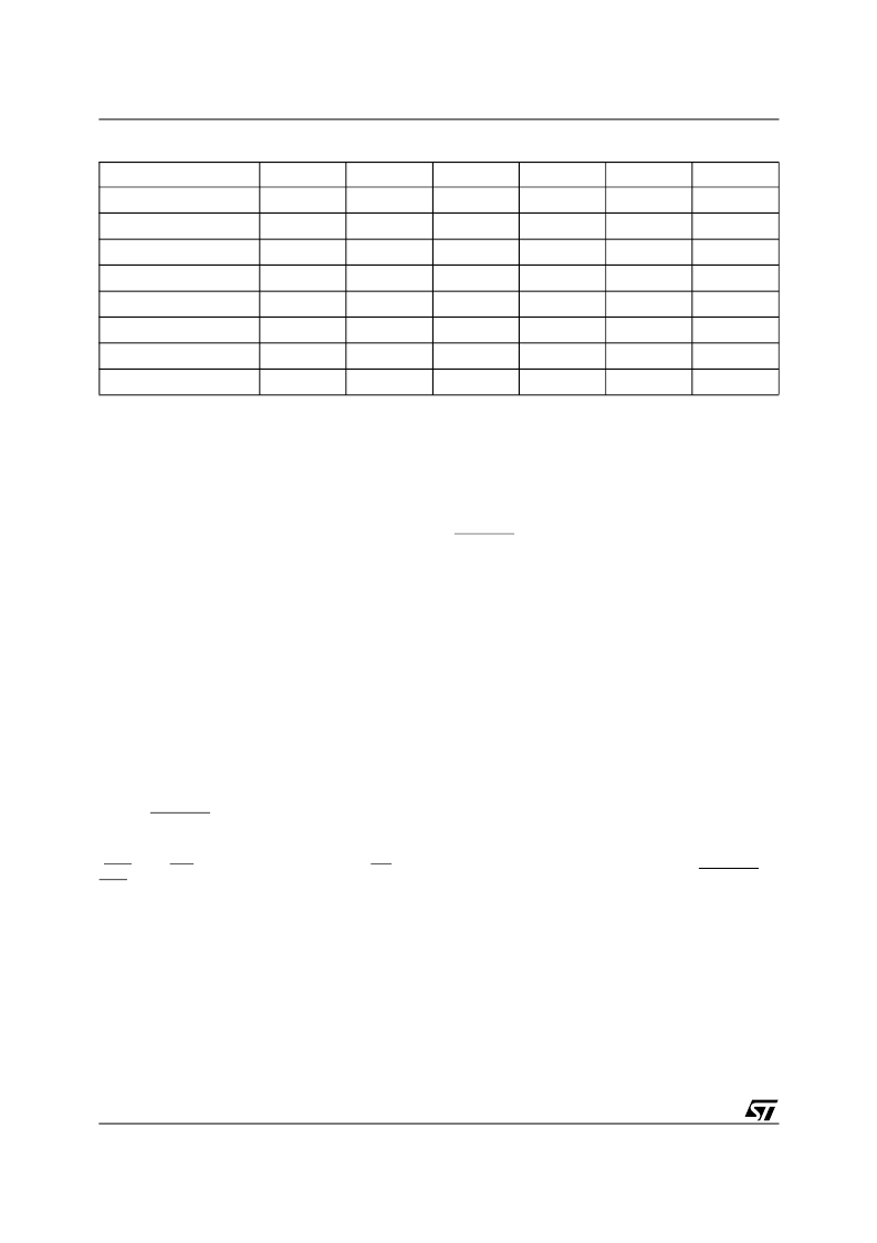
Table 5. Memory Identification Input Configuration (LPC mode)
BUS OPERATIONS
The two interfaces, A/A Mux and FWH/LPC, sup-
port similar operations, but with different bus sig-
nals and timings. The Firmware Hub/Low Pin
Count (FWH/LPC) Interface offers full functional-
ity, while the Address/Address Multiplexed (A/A
Mux) Interface is orientated for erase and program
operations.
See the sections below, The
Firmware Hub/Low
Pin Count (FWH/LPC) Bus Operations
and
Ad-
dress/Address Multiplexed (A/A Mux) Bus Opera-
tions
, for details of the bus operations on each
interface.
Firmware Hub/Low Pin Count (FWH/LPC) Bus
Operations
The M50FLW040 automatically identifies the type
of FWH/LPC protocol from the first received nibble
(START nibble) and decodes the data that it re-
ceives afterwards, according to the chosen FWH
or LPC mode. The Firmware Hub/Low Pin Count
(FWH/LPC) Interface consists of four data signals
(FWH0/LAD0-FWH3/LAD3), one control line
(FWH4/LFRAME) and a clock (CLK).
Protection against accidental or malicious data
corruption is achieved using two additional signals
(TBL and WP). And two reset signals (RP and
INIT) are available to put the memory into a known
state.
The data, control and clock signals are designed
to be compatible with PCI electrical specifications.
The interface operates with clock speeds of up to
33MHz.
The following operations can be performed using
the appropriate bus cycles: Bus Read, Bus Write,
Standby, Reset and Block Protection.
Bus Read.
Bus Read operations are used to read
from the memory cells, specific registers in the
Command Interface or Firmware Hub/Low Pin
Count Registers. A valid Bus Read operation
starts on the rising edge of the Clock signal when
the
Input
Communication
LFRAME, is Low, V
IL
, and the correct Start cycle
is present on FWH0/LAD0-FWH3/LAD3. On sub-
sequent clock cycles the Host will send to the
memory:
ID Select, Address and other control bits on
FWH0-FWH3 in FWH mode.
Type+Dir Address and other control bits on
LAD0-LAD3 in LPC mode.
The device responds by outputting Sync data until
the wait states have elapsed, followed by Data0-
Data3 and Data4-Data7.
See
Table 6.
and
Table 8.
, and
Figure 7.
and
Fig-
ure 9.
, for a description of the Field definitions for
each clock cycle of the transfer. See
Table 26.
,
and
Figure 15.
, for details on the timings of the sig-
nals.
Bus Write.
Bus Write operations are used to write
to the Command Interface or Firmware Hub/Low
Pin Count Registers. A valid Bus Write operation
starts on the rising edge of the Clock signal when
Input Communication Frame, FWH4/LFRAME, is
Low, V
IL
, and the correct Start cycle is present on
FWH0/LAD0-FWH3/LAD3. On subsequent Clock
cycles the Host will send to the memory:
ID Select, Address, other control bits, Data0-
Data3 and Data4-Data7 on FWH0-FWH3 in
FWH mode.
Cycle Type + Dir, Address, other control bits,
Data0-Data3 and Data4-Data7 on LAD0-
LAD3.
The device responds by outputting Sync data until
the wait states have elapsed.
Frame,
FWH4/
I
I
I
I
Memory Number
ID2
ID1
ID0
A21
A20
A19
1 (Boot memory)
V
IL
or float
V
IL
or float
V
IL
or float
1
1
1
2
V
IL
or float
V
IL
or float
V
IH
1
1
0
3
V
IL
or float
V
IH
V
IL
or float
1
0
1
4
V
IL
or float
V
IH
V
IH
1
0
0
5
V
IH
V
IL
or float
V
IL
or float
0
1
1
6
V
IH
V
IL
or float
V
IH
0
1
0
7
V
IH
V
IH
V
IL
or float
0
0
1
8
V
IH
V
IH
V
IH
0
0
0
相關(guān)PDF資料 |
PDF描述 |
|---|---|
| M50FLW040BNB1 | 4 Mbit (5 x 64KByte Blocks + 3 x 16 x 4KByte Sectors) 3V Supply Firmware Hub / Low Pin Count Flash Memory |
| M50FLW040BNB1G | 4 Mbit (5 x 64KByte Blocks + 3 x 16 x 4KByte Sectors) 3V Supply Firmware Hub / Low Pin Count Flash Memory |
| M50FLW040BNB1P | 4 Mbit (5 x 64KByte Blocks + 3 x 16 x 4KByte Sectors) 3V Supply Firmware Hub / Low Pin Count Flash Memory |
| M50FLW040BNB1T | 4 Mbit (5 x 64KByte Blocks + 3 x 16 x 4KByte Sectors) 3V Supply Firmware Hub / Low Pin Count Flash Memory |
| M50FLW040BNB1TG | 4 Mbit (5 x 64KByte Blocks + 3 x 16 x 4KByte Sectors) 3V Supply Firmware Hub / Low Pin Count Flash Memory |
相關(guān)代理商/技術(shù)參數(shù) |
參數(shù)描述 |
|---|---|
| M50FLW040BNB1 | 制造商:STMICROELECTRONICS 制造商全稱:STMicroelectronics 功能描述:4 Mbit (5 x 64KByte Blocks + 3 x 16 x 4KByte Sectors) 3V Supply Firmware Hub / Low Pin Count Flash Memory |
| M50FLW040BNB1G | 制造商:STMICROELECTRONICS 制造商全稱:STMicroelectronics 功能描述:4 Mbit (5 x 64KByte Blocks + 3 x 16 x 4KByte Sectors) 3V Supply Firmware Hub / Low Pin Count Flash Memory |
| M50FLW040BNB1P | 制造商:STMICROELECTRONICS 制造商全稱:STMicroelectronics 功能描述:4 Mbit (5 x 64KByte Blocks + 3 x 16 x 4KByte Sectors) 3V Supply Firmware Hub / Low Pin Count Flash Memory |
| M50FLW040BNB1T | 制造商:STMICROELECTRONICS 制造商全稱:STMicroelectronics 功能描述:4 Mbit (5 x 64KByte Blocks + 3 x 16 x 4KByte Sectors) 3V Supply Firmware Hub / Low Pin Count Flash Memory |
| M50FLW040BNB1TG | 制造商:STMICROELECTRONICS 制造商全稱:STMicroelectronics 功能描述:4 Mbit (5 x 64KByte Blocks + 3 x 16 x 4KByte Sectors) 3V Supply Firmware Hub / Low Pin Count Flash Memory |
發(fā)布緊急采購,3分鐘左右您將得到回復(fù)。