- 您現(xiàn)在的位置:買(mǎi)賣(mài)IC網(wǎng) > PDF目錄377829 > M50FLW040BN5T (意法半導(dǎo)體) 4 Mbit (5 x 64KByte Blocks + 3 x 16 x 4KByte Sectors) 3V Supply Firmware Hub / Low Pin Count Flash Memory PDF資料下載
參數(shù)資料
| 型號(hào): | M50FLW040BN5T |
| 廠商: | 意法半導(dǎo)體 |
| 英文描述: | 4 Mbit (5 x 64KByte Blocks + 3 x 16 x 4KByte Sectors) 3V Supply Firmware Hub / Low Pin Count Flash Memory |
| 中文描述: | 4兆位(5 × 64KB之座3 × 16 × 4KB的部門(mén))3V電源固件集線器/低引腳數(shù)快閃記憶體 |
| 文件頁(yè)數(shù): | 15/52頁(yè) |
| 文件大小: | 417K |
| 代理商: | M50FLW040BN5T |
第1頁(yè)第2頁(yè)第3頁(yè)第4頁(yè)第5頁(yè)第6頁(yè)第7頁(yè)第8頁(yè)第9頁(yè)第10頁(yè)第11頁(yè)第12頁(yè)第13頁(yè)第14頁(yè)當(dāng)前第15頁(yè)第16頁(yè)第17頁(yè)第18頁(yè)第19頁(yè)第20頁(yè)第21頁(yè)第22頁(yè)第23頁(yè)第24頁(yè)第25頁(yè)第26頁(yè)第27頁(yè)第28頁(yè)第29頁(yè)第30頁(yè)第31頁(yè)第32頁(yè)第33頁(yè)第34頁(yè)第35頁(yè)第36頁(yè)第37頁(yè)第38頁(yè)第39頁(yè)第40頁(yè)第41頁(yè)第42頁(yè)第43頁(yè)第44頁(yè)第45頁(yè)第46頁(yè)第47頁(yè)第48頁(yè)第49頁(yè)第50頁(yè)第51頁(yè)第52頁(yè)
15/52
M50FLW040A, M50FLW040B
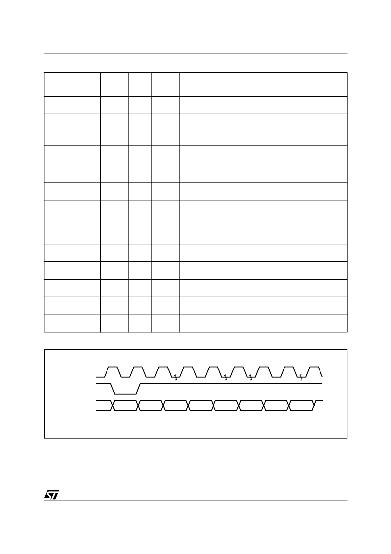
Table 7. FWH Bus Write Field Definitions
Figure 8. FWH Bus Write Waveforms
Clock
Cycle
Number
Clock
Cycle
Count
Field
FWH0-
FWH3
Memory
I/O
Description
1
1
START
1110b
I
On the rising edge of CLK with FWH4 Low, the contents of
FWH0-FWH3 indicate the start of a FWH Write Cycle.
2
1
IDSEL
XXXX
I
Indicates which FWH Flash Memory is selected. The value on
FWH0-FWH3 is compared to the IDSEL strapping on the FWH
Flash Memory pins to select which FWH Flash Memory is being
addressed.
3-9
7
ADDR
XXXX
I
A 28-bit address is transferred, with the most significant nibble
first. Address lines A19-21 and A23-27 are treated as Don
’
t
Care during a normal memory array access, with A22=1, but are
taken into account for a register access, with A22=0. (See
Table
15.
)
10
1
MSIZE
XXXX
I
0000(Single Byte Transfer) 0001 (Double Byte Transfer) 0010b
(Quadruple Byte Transfer).
11-18
M=2/4/8
DATA
XXXX
I
Data transfer is two cycles, starting with the least significant
nibble. (The first pair of nibbles is that at the address with A1-
A0 set to 00, the second pair with A1-A0 set to 01, the third
pair with A1-A0 set to 10, and the fourth pair with A1-A0 set
to 11. In Double Byte Program the first pair of nibbles is that at
the address with A0 set to 0, the second pair with A0 set to 1)
previous
+1
1
TAR
1111b
I
The host drives FWH0-FWH3 to 1111b to indicate a turnaround
cycle.
previous
+1
1
TAR
1111b
(float)
O
The FWH Flash Memory takes control of FWH0-FWH3 during
this cycle.
previous
+1
1
SYNC
0000b
O
The FWH Flash Memory drives FWH0-FWH3 to 0000b,
indicating it has received data or a command.
previous
+1
1
TAR
1111b
O
The FWH Flash Memory drives FWH0-FWH3 to 1111b,
indicating a turnaround cycle.
previous
+1
1
TAR
1111b
(float)
N/A
The FWH Flash Memory floats its outputs and the host takes
control of FWH0-FWH3.
AI08434B
CLK
FWH4
FWH0-FWH3
Number of
clock cycles
START
IDSEL
ADDR
MSIZE
DATA
TAR
SYNC
TAR
1
1
7
1
M
2
1
2
相關(guān)PDF資料 |
PDF描述 |
|---|---|
| M50FLW040BN5TG | 4 Mbit (5 x 64KByte Blocks + 3 x 16 x 4KByte Sectors) 3V Supply Firmware Hub / Low Pin Count Flash Memory |
| M50FLW040BN5TP | 4 Mbit (5 x 64KByte Blocks + 3 x 16 x 4KByte Sectors) 3V Supply Firmware Hub / Low Pin Count Flash Memory |
| M50FLW040BNB1 | 4 Mbit (5 x 64KByte Blocks + 3 x 16 x 4KByte Sectors) 3V Supply Firmware Hub / Low Pin Count Flash Memory |
| M50FLW040BNB1G | 4 Mbit (5 x 64KByte Blocks + 3 x 16 x 4KByte Sectors) 3V Supply Firmware Hub / Low Pin Count Flash Memory |
| M50FLW040BNB1P | 4 Mbit (5 x 64KByte Blocks + 3 x 16 x 4KByte Sectors) 3V Supply Firmware Hub / Low Pin Count Flash Memory |
相關(guān)代理商/技術(shù)參數(shù) |
參數(shù)描述 |
|---|---|
| M50FLW040BN5TG | 制造商:STMICROELECTRONICS 制造商全稱(chēng):STMicroelectronics 功能描述:4 Mbit (5 x 64KByte Blocks + 3 x 16 x 4KByte Sectors) 3V Supply Firmware Hub / Low Pin Count Flash Memory |
| M50FLW040BN5TP | 制造商:STMICROELECTRONICS 制造商全稱(chēng):STMicroelectronics 功能描述:4 Mbit (5 x 64KByte Blocks + 3 x 16 x 4KByte Sectors) 3V Supply Firmware Hub / Low Pin Count Flash Memory |
| M50FLW040BNB1 | 制造商:STMICROELECTRONICS 制造商全稱(chēng):STMicroelectronics 功能描述:4 Mbit (5 x 64KByte Blocks + 3 x 16 x 4KByte Sectors) 3V Supply Firmware Hub / Low Pin Count Flash Memory |
| M50FLW040BNB1G | 制造商:STMICROELECTRONICS 制造商全稱(chēng):STMicroelectronics 功能描述:4 Mbit (5 x 64KByte Blocks + 3 x 16 x 4KByte Sectors) 3V Supply Firmware Hub / Low Pin Count Flash Memory |
| M50FLW040BNB1P | 制造商:STMICROELECTRONICS 制造商全稱(chēng):STMicroelectronics 功能描述:4 Mbit (5 x 64KByte Blocks + 3 x 16 x 4KByte Sectors) 3V Supply Firmware Hub / Low Pin Count Flash Memory |
發(fā)布緊急采購(gòu),3分鐘左右您將得到回復(fù)。