- 您現(xiàn)在的位置:買賣IC網(wǎng) > PDF目錄377828 > M50FLW040ANB5G (意法半導(dǎo)體) 4 Mbit (5 x 64KByte Blocks + 3 x 16 x 4KByte Sectors) 3V Supply Firmware Hub / Low Pin Count Flash Memory PDF資料下載
參數(shù)資料
| 型號(hào): | M50FLW040ANB5G |
| 廠商: | 意法半導(dǎo)體 |
| 英文描述: | 4 Mbit (5 x 64KByte Blocks + 3 x 16 x 4KByte Sectors) 3V Supply Firmware Hub / Low Pin Count Flash Memory |
| 中文描述: | 4兆位(5 × 64KB之座3 × 16 × 4KB的部門)3V電源固件集線器/低引腳數(shù)快閃記憶體 |
| 文件頁(yè)數(shù): | 24/52頁(yè) |
| 文件大小: | 417K |
| 代理商: | M50FLW040ANB5G |
第1頁(yè)第2頁(yè)第3頁(yè)第4頁(yè)第5頁(yè)第6頁(yè)第7頁(yè)第8頁(yè)第9頁(yè)第10頁(yè)第11頁(yè)第12頁(yè)第13頁(yè)第14頁(yè)第15頁(yè)第16頁(yè)第17頁(yè)第18頁(yè)第19頁(yè)第20頁(yè)第21頁(yè)第22頁(yè)第23頁(yè)當(dāng)前第24頁(yè)第25頁(yè)第26頁(yè)第27頁(yè)第28頁(yè)第29頁(yè)第30頁(yè)第31頁(yè)第32頁(yè)第33頁(yè)第34頁(yè)第35頁(yè)第36頁(yè)第37頁(yè)第38頁(yè)第39頁(yè)第40頁(yè)第41頁(yè)第42頁(yè)第43頁(yè)第44頁(yè)第45頁(yè)第46頁(yè)第47頁(yè)第48頁(yè)第49頁(yè)第50頁(yè)第51頁(yè)第52頁(yè)
M50FLW040A, M50FLW040B
24/52
FIRMWARE HUB/LOW PIN COUNT (FWH/LPC) INTERFACE CONFIGURATION
REGISTERS
When the Firmware Hub Interface/Low Pin Count
is selected, several additional registers can be ac-
cessed. These registers control the protection sta-
tus of the Blocks, read the General Purpose Input
pins and identify the memory using the manufac-
turer code. See
Table 15.
for the memory map of
the Configuration Registers. The Configuration
registers are accessed directly without using any
specific command code. A single Bus Write or Bus
Read Operation, with the appropriate address (in-
cluding A22=0), is all that is needed.
Lock Registers
The Lock Registers control the protection status of
the Blocks. Each Block has its own Lock Register.
Three bits within each Lock Register control the
protection of each block: the Write Lock Bit, the
Read Lock Bit and the Lock Down Bit.
The Lock Registers can be read and written. Care
should be taken, though, when writing. Once the
Lock Down Bit is set,
‘
1
’
, further modifications to
the Lock Register cannot be made until it is
cleared again by a reset or power-up.
See
Table 16.
for details on the bit definitions of
the Lock Registers.
Write Lock.
The Write Lock Bit determines
whether the contents of the Block can be modified
(using the Program or Erase Command). When
the Write Lock Bit is set,
‘
1
’
, the block is write pro-
tected
–
any operations that attempt to change the
data in the block will fail, and the Status Register
will report the error. When the Write Lock Bit is re-
set,
‘
0
’
, the block is not write protected by the Lock
Register, and may be modified, unless it is write
protected by some other means.
If the Top Block Lock signal, TBL, is Low, V
IL
, then
the Top Block (Block 7) is write protected, and
cannot be modified. Similarly, if the Write Protect
signal, WP, is Low, V
IL
, then the Main Blocks
(Blocks 0 to 6) are write protected, and cannot be
modified.
After power-up, or reset, the Write Lock Bit is al-
ways set to
‘
1
’
(write-protected).
Read Lock.
The Read Lock bit determines
whether the contents of the Block can be read (in
Read mode). When the Read Lock Bit is set,
‘
1
’
,
the block is read protected
–
any operation that at-
tempts to read the contents of the block will read
00h instead. When the Read Lock Bit is reset,
‘
0
’
,
read operations are allowed in the Block, and re-
turn the value of the data that had been pro-
grammed in the block.
After power-up, or reset, the Read Lock Bit is al-
ways reset to
‘
0
’
(not read-protected).
Lock Down.
The Lock Down Bit provides a
mechanism for protecting software data from sim-
ple hacking and malicious attack. When the Lock
Down Bit is set,
‘
1
’
, further modification to the
Write Lock, Read Lock and Lock Down Bits cannot
be performed. A reset, or power-up, is required be-
fore changes to these bits can be made. When the
Lock Down Bit is reset,
‘
0
’
, the Write Lock, Read
Lock and Lock Down Bits can be changed.
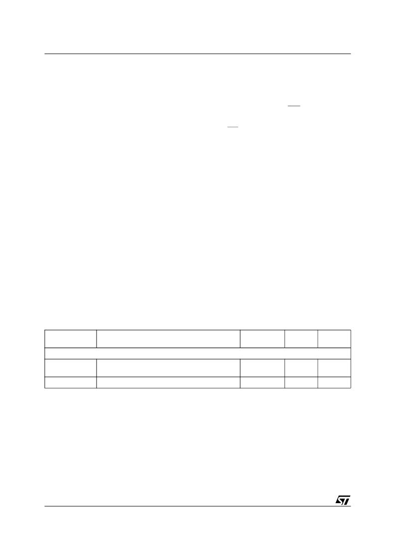
Table 15. Configuration Register Map
Note: In LPC mode, a most significant nibble, F, must be added to the memory address. For all registers, A22=0, and the remaining address
bits should be set according to the rules shown in the ADDR field of
Table 6.
to
Table 9.
.
Mnemonic
Register Name
Memory
Address
Default
Value
Access
Lock Registers (For details, see
APPENDIX A.
)
GPI_REG
Firmware Hub/Low Pin Count (FWH/LPC) General
Purpose Input Register
FBC0100h
N/A
R
MANU_REG
Manufacturer Code Register
FBC0000h
20h
R
相關(guān)PDF資料 |
PDF描述 |
|---|---|
| M50FLW040ANB5P | 4 Mbit (5 x 64KByte Blocks + 3 x 16 x 4KByte Sectors) 3V Supply Firmware Hub / Low Pin Count Flash Memory |
| M50FLW040ANB5T | 4 Mbit (5 x 64KByte Blocks + 3 x 16 x 4KByte Sectors) 3V Supply Firmware Hub / Low Pin Count Flash Memory |
| M50FLW040ANB5TG | 4 Mbit (5 x 64KByte Blocks + 3 x 16 x 4KByte Sectors) 3V Supply Firmware Hub / Low Pin Count Flash Memory |
| M50FLW040ANB5TP | 4 Mbit (5 x 64KByte Blocks + 3 x 16 x 4KByte Sectors) 3V Supply Firmware Hub / Low Pin Count Flash Memory |
| M50FLW040B | 4 Mbit (5 x 64KByte Blocks + 3 x 16 x 4KByte Sectors) 3V Supply Firmware Hub / Low Pin Count Flash Memory |
相關(guān)代理商/技術(shù)參數(shù) |
參數(shù)描述 |
|---|---|
| M50FLW040ANB5P | 制造商:STMICROELECTRONICS 制造商全稱:STMicroelectronics 功能描述:4 Mbit (5 x 64KByte Blocks + 3 x 16 x 4KByte Sectors) 3V Supply Firmware Hub / Low Pin Count Flash Memory |
| M50FLW040ANB5T | 制造商:STMICROELECTRONICS 制造商全稱:STMicroelectronics 功能描述:4 Mbit (5 x 64KByte Blocks + 3 x 16 x 4KByte Sectors) 3V Supply Firmware Hub / Low Pin Count Flash Memory |
| M50FLW040ANB5TG | 功能描述:閃存 SERIAL FLASH RoHS:否 制造商:ON Semiconductor 數(shù)據(jù)總線寬度:1 bit 存儲(chǔ)類型:Flash 存儲(chǔ)容量:2 MB 結(jié)構(gòu):256 K x 8 定時(shí)類型: 接口類型:SPI 訪問(wèn)時(shí)間: 電源電壓-最大:3.6 V 電源電壓-最小:2.3 V 最大工作電流:15 mA 工作溫度:- 40 C to + 85 C 安裝風(fēng)格:SMD/SMT 封裝 / 箱體: 封裝:Reel |
| M50FLW040ANB5TP | 制造商:STMICROELECTRONICS 制造商全稱:STMicroelectronics 功能描述:4 Mbit (5 x 64KByte Blocks + 3 x 16 x 4KByte Sectors) 3V Supply Firmware Hub / Low Pin Count Flash Memory |
| M50FLW040B | 制造商:STMICROELECTRONICS 制造商全稱:STMicroelectronics 功能描述:4 Mbit (5 x 64KByte Blocks + 3 x 16 x 4KByte Sectors) 3V Supply Firmware Hub / Low Pin Count Flash Memory |
發(fā)布緊急采購(gòu),3分鐘左右您將得到回復(fù)。