- 您現(xiàn)在的位置:買賣IC網(wǎng) > PDF目錄377828 > M50FLW040AK1T (意法半導(dǎo)體) 4 Mbit (5 x 64KByte Blocks + 3 x 16 x 4KByte Sectors) 3V Supply Firmware Hub / Low Pin Count Flash Memory PDF資料下載
參數(shù)資料
| 型號: | M50FLW040AK1T |
| 廠商: | 意法半導(dǎo)體 |
| 英文描述: | 4 Mbit (5 x 64KByte Blocks + 3 x 16 x 4KByte Sectors) 3V Supply Firmware Hub / Low Pin Count Flash Memory |
| 中文描述: | 4兆位(5 × 64KB之座3 × 16 × 4KB的部門)3V電源固件集線器/低引腳數(shù)快閃記憶體 |
| 文件頁數(shù): | 16/52頁 |
| 文件大小: | 417K |
| 代理商: | M50FLW040AK1T |
第1頁第2頁第3頁第4頁第5頁第6頁第7頁第8頁第9頁第10頁第11頁第12頁第13頁第14頁第15頁當前第16頁第17頁第18頁第19頁第20頁第21頁第22頁第23頁第24頁第25頁第26頁第27頁第28頁第29頁第30頁第31頁第32頁第33頁第34頁第35頁第36頁第37頁第38頁第39頁第40頁第41頁第42頁第43頁第44頁第45頁第46頁第47頁第48頁第49頁第50頁第51頁第52頁
M50FLW040A, M50FLW040B
16/52
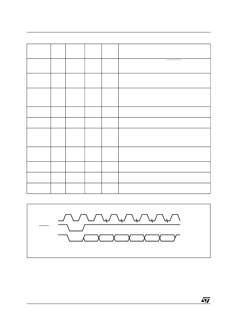
Table 8. LPC Bus Read Field Definitions (1-Byte)
Figure 9. LPC Bus Read Waveforms (1-Byte)
Clock Cycle
Number
Clock
Cycle
Count
Field
LAD0-
LAD3
Memory
I/O
Description
1
1
START
0000b
I
On the rising edge of CLK with LFRAME Low, the contents
of LAD0-LAD3 must be 0000b to indicate the start of a
LPC cycle.
2
1
CYCTYPE
+ DIR
0100b
I
Indicates the type of cycle and selects 1-byte reading. Bits
3:2 must be 01b. Bit 1 indicates the direction of transfer: 0b
for read. Bit 0 is Don
’
t Care.
3-10
8
ADDR
XXXX
I
A 32-bit address is transferred, with the most significant
nibble first. A23-A31 must be set to 1. A22=1 for memory
access, and A22=0 for register access.
Table 5.
shows the
appropriate values for A21-A19.
11
1
TAR
1111b
I
The host drives LAD0-LAD3 to 1111b to indicate a
turnaround cycle.
12
1
TAR
1111b
(float)
O
The LPC Flash Memory takes control of LAD0-LAD3
during this cycle.
13-14
2
WSYNC
0101b
O
The LPC Flash Memory drives LAD0-LAD3 to 0101b
(short wait-sync) for two clock cycles, indicating that the
data is not yet available. Two wait-states are always
included.
15
1
RSYNC
0000b
O
The LPC Flash Memory drives LAD0-LAD3 to 0000b,
indicating that data will be available during the next clock
cycle.
16-17
2
DATA
XXXX
O
Data transfer is two CLK cycles, starting with the least
significant nibble.
18
1
TAR
1111b
O
The LPC Flash Memory drives LAD0-LAD3 to 1111b to
indicate a turnaround cycle.
19
1
TAR
1111b
(float)
N/A
The LPC Flash Memory floats its outputs, the host takes
control of LAD0-LAD3.
AI04429
CLK
LFRAME
LAD0-LAD3
Number of
clock cycles
START
CYCTYPE
+ DIR
ADDR
TAR
SYNC
DATA
TAR
1
1
8
2
3
2
2
相關(guān)PDF資料 |
PDF描述 |
|---|---|
| M50FLW040AK1TG | 4 Mbit (5 x 64KByte Blocks + 3 x 16 x 4KByte Sectors) 3V Supply Firmware Hub / Low Pin Count Flash Memory |
| M50FLW040AK1TP | 4 Mbit (5 x 64KByte Blocks + 3 x 16 x 4KByte Sectors) 3V Supply Firmware Hub / Low Pin Count Flash Memory |
| M50FLW040AK5 | 4 Mbit (5 x 64KByte Blocks + 3 x 16 x 4KByte Sectors) 3V Supply Firmware Hub / Low Pin Count Flash Memory |
| M50FLW040AK5T | 4 Mbit (5 x 64KByte Blocks + 3 x 16 x 4KByte Sectors) 3V Supply Firmware Hub / Low Pin Count Flash Memory |
| M50FLW040AN1 | 4 Mbit (5 x 64KByte Blocks + 3 x 16 x 4KByte Sectors) 3V Supply Firmware Hub / Low Pin Count Flash Memory |
相關(guān)代理商/技術(shù)參數(shù) |
參數(shù)描述 |
|---|---|
| M50FLW040AK1TG | 制造商:STMICROELECTRONICS 制造商全稱:STMicroelectronics 功能描述:4 Mbit (5 x 64KByte Blocks + 3 x 16 x 4KByte Sectors) 3V Supply Firmware Hub / Low Pin Count Flash Memory |
| M50FLW040AK1TP | 制造商:STMICROELECTRONICS 制造商全稱:STMicroelectronics 功能描述:4 Mbit (5 x 64KByte Blocks + 3 x 16 x 4KByte Sectors) 3V Supply Firmware Hub / Low Pin Count Flash Memory |
| M50FLW040AK5 | 制造商:STMICROELECTRONICS 制造商全稱:STMicroelectronics 功能描述:4 Mbit (5 x 64KByte Blocks + 3 x 16 x 4KByte Sectors) 3V Supply Firmware Hub / Low Pin Count Flash Memory |
| M50FLW040AK5G | 功能描述:閃存 SERIAL FLASH RoHS:否 制造商:ON Semiconductor 數(shù)據(jù)總線寬度:1 bit 存儲類型:Flash 存儲容量:2 MB 結(jié)構(gòu):256 K x 8 定時類型: 接口類型:SPI 訪問時間: 電源電壓-最大:3.6 V 電源電壓-最小:2.3 V 最大工作電流:15 mA 工作溫度:- 40 C to + 85 C 安裝風格:SMD/SMT 封裝 / 箱體: 封裝:Reel |
| M50FLW040AK5P | 制造商:STMICROELECTRONICS 制造商全稱:STMicroelectronics 功能描述:4-Mbit (5 】 64 Kbyte blocks + 3 】 16 】 4 Kbyte sectors) 3-V supply Firmware Hub / low-pin count Flash memory |
發(fā)布緊急采購,3分鐘左右您將得到回復(fù)。