- 您現(xiàn)在的位置:買賣IC網(wǎng) > PDF目錄377826 > M41ST84WMQ6 (意法半導(dǎo)體) 3.0/3.3V I2C Serial RTC with Supervisory Functions PDF資料下載
參數(shù)資料
| 型號: | M41ST84WMQ6 |
| 廠商: | 意法半導(dǎo)體 |
| 英文描述: | 3.0/3.3V I2C Serial RTC with Supervisory Functions |
| 中文描述: | 3.0/3.3V I2C串行實時時鐘具有監(jiān)督職能 |
| 文件頁數(shù): | 12/29頁 |
| 文件大小: | 176K |
| 代理商: | M41ST84WMQ6 |
第1頁第2頁第3頁第4頁第5頁第6頁第7頁第8頁第9頁第10頁第11頁當前第12頁第13頁第14頁第15頁第16頁第17頁第18頁第19頁第20頁第21頁第22頁第23頁第24頁第25頁第26頁第27頁第28頁第29頁
M41ST84W
12/29
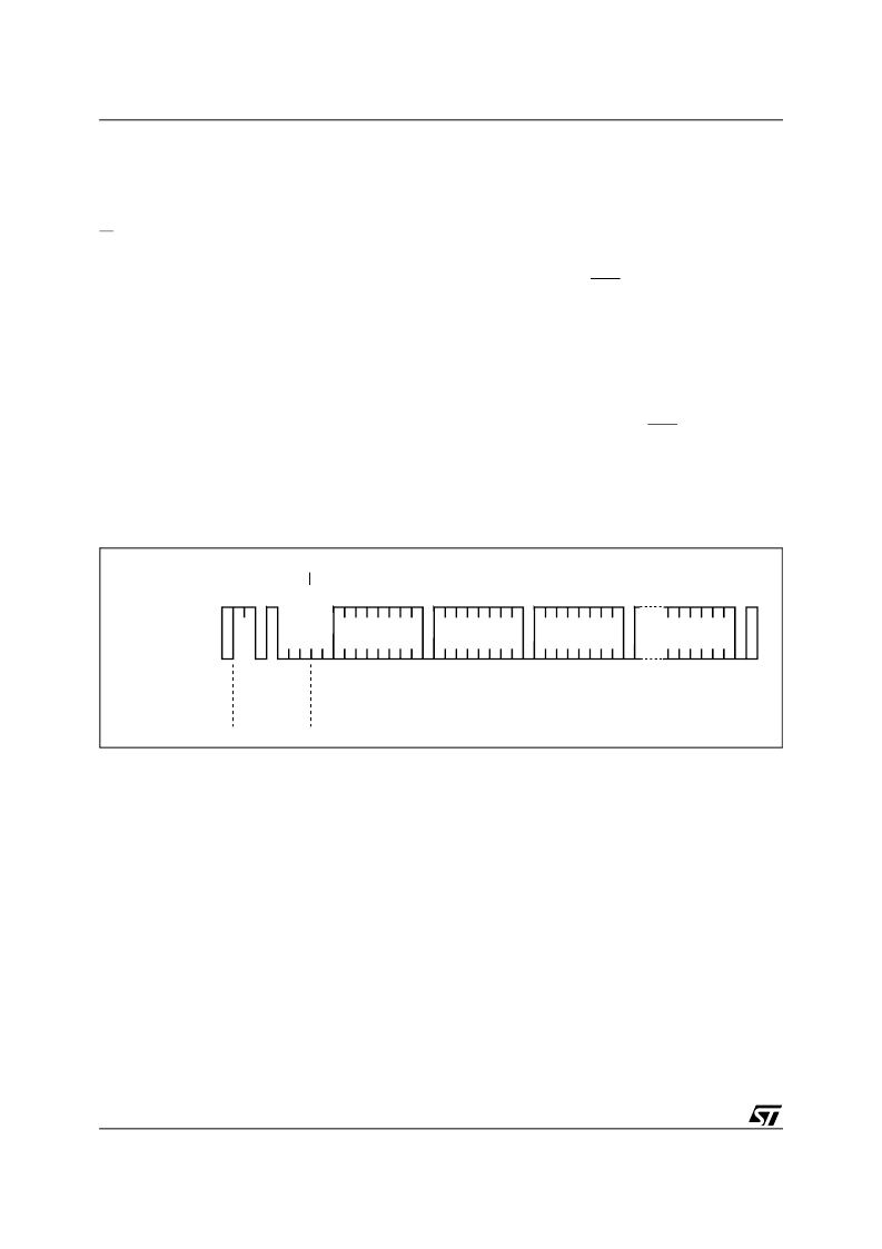
WRITE Mode
In this mode the master transmitter transmits to
the M41ST84W slave receiver. Bus protocol is
shown in
Figure 12., page 12
. Following the
START condition and slave address, a logic '0' (R/
W=0) is placed on the bus and indicates to the ad-
dressed device that word address An will follow
and is to be written to the on-chip address pointer.
The data word to be written to the memory is
strobed in next and the internal address pointer is
incremented to the next memory location within
the RAM on the reception of an acknowledge
clock. The M41ST84W slave receiver will send an
acknowledge clock to the master transmitter after
it has received the slave address (see
Figure
9., page 10
) and again after it has received the
word address and each data byte.
Data Retention Mode
With valid V
CC
applied, the M41ST84W can be ac-
cessed as described above with READ or WRITE
cycles. Should the supply voltage decay, the
M41ST84W will automatically deselect, write pro-
tecting itself when V
CC
falls between V
PFD
(max)
and V
PFD
(min). This is accomplished by internally
inhibiting access to the clock registers. At this
time, the Reset pin (RST) is driven active and will
remain active until V
CC
returns to nominal levels.
When V
CC
falls below the Battery Back-up
Switchover Voltage (V
SO
), power input is switched
from the V
CC
pin to the external battery, and the
clock registers and SRAM are maintained from the
attached battery supply.
All outputs become high impedance. On power up,
when V
CC
returns to a nominal value, write protec-
tion continues for t
rec
. The RST signal also re-
mains active during this time (see
Figure
19., page 25
).
For a further more detailed review of lifetime calcu-
lations, please see Application Note AN1012.
Figure 12. WRITE Mode Sequence
AI00591
BUS ACTIVITY:
A
S
A
A
A
A
S
S
P
SDA LINE
BUS ACTIVITY:
MASTER
R
DATA n
DATA n+1
DATA n+X
WORD
ADDRESS (An)
SLAVE
ADDRESS
發(fā)布緊急采購,3分鐘左右您將得到回復(fù)。