- 您現(xiàn)在的位置:買賣IC網(wǎng) > PDF目錄377825 > M40Z300AVMH1F (意法半導(dǎo)體) 3V NVRAM Supervisor for Up to 8 LPSRAMs PDF資料下載
參數(shù)資料
| 型號: | M40Z300AVMH1F |
| 廠商: | 意法半導(dǎo)體 |
| 英文描述: | 3V NVRAM Supervisor for Up to 8 LPSRAMs |
| 中文描述: | 3V的NVRAM中監(jiān)多達(dá)8個LPSRAMs |
| 文件頁數(shù): | 6/20頁 |
| 文件大小: | 131K |
| 代理商: | M40Z300AVMH1F |
M40Z300AV
6/20
OPERATION
The M40Z300AV, as shown in
Figure 6., page 5
,
can control up to four (eight, if placed in parallel)
standard low-power SRAMs. These SRAMs must
be configured to have the chip enable input dis-
able all other input signals. Most slow, low-power
SRAMs are configured like this, however many
fast SRAMs are not. During normal operating con-
ditions, the conditioned chip enable (E1
CON
to
E4
CON
) output pins follow the chip enable (E) input
pin with timing shown in
Figure 7., page 6
and
Ta-
ble 7., page 13
. An internal switch connects V
CC
to V
OUT
. This switch has a voltage drop of less
than 0.3V (I
OUT1
).
When V
CC
degrades during a power failure,
E1
CON
to E4
CON
are forced inactive independent
of E. In this situation, the SRAM is unconditionally
write protected as V
CC
falls below an out-of-toler-
ance threshold (V
PFD
). For the M40Z300AV, the
THS pin must be tied to ground (as shown in
Table
6., page 11
).
If chip enable access is in progress during a power
fail detection, that memory cycle continues to com-
pletion before the memory is write protected. If the
memory cycle is not terminated within time t
WPT
,
E1
CON
to E4
CON
are unconditionally driven high,
write protecting the SRAM. A power failure during
a WRITE cycle may corrupt data at the currently
addressed location, but does not jeopardize the
rest of the SRAM's contents. At voltages below
V
PFD
(min), the user can be assured the memory
will be write protected within the Write Protect
Time (t
WPT
) provided the V
CC
fall time exceeds t
F
(see
Figure 7., page 6
).
As V
CC
continues to degrade, the internal switch
disconnects V
CC
and connects the internal battery
to V
OUT
. This occurs at the switchover voltage
(V
SO
). Below the V
SO
, the battery provides a volt-
age V
OHB
to the SRAM and can supply current
I
OUT2
(see
Table 6., page 11
).
When V
CC
rises above V
SO
, V
OUT
is switched
back to the supply voltage. Outputs E1
CON
to
E4
CON
are held inactive for t
CER
(120ms maxi-
mum) after the power supply has reached V
PFD
,
independent of the E input, to allow for processor
stabilization (see
Figure 11., page 12
).
Two to Four Decode
The M40Z300AV includes a 2 input (A, B) decoder
which allows the control of up to 4 independent
SRAMs. The Truth Table for these inputs is shown
in Table
2
.
Table 2. Truth Table
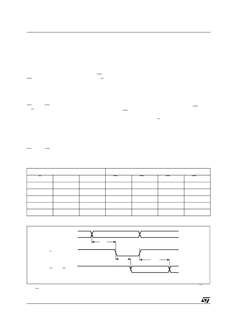
Figure 7. Address-Decode Time
Note: During system design, compliance with the SRAM timing parameters must comprehend the propagation delay between E1
CON
-
E4
CON
.
Inputs
Outputs
E
B
A
E1
CON
E2
CON
E3
CON
E4
CON
H
X
X
H
H
H
H
L
L
L
L
H
H
H
L
L
H
H
L
H
H
L
H
L
H
H
L
H
L
H
H
H
H
H
L
AI02551
A, B
E
E1CON - E4CON
tAS
tEDH
tEDL
相關(guān)PDF資料 |
PDF描述 |
|---|---|
| M40Z300AVMH6E | 3V NVRAM Supervisor for Up to 8 LPSRAMs |
| M40Z300AVMH6F | 3V NVRAM Supervisor for Up to 8 LPSRAMs |
| M40Z300AVMQ1E | 3V NVRAM Supervisor for Up to 8 LPSRAMs |
| M40Z300AVMQ1F | 3V NVRAM Supervisor for Up to 8 LPSRAMs |
| M40Z300AVMQ6E | 3V NVRAM Supervisor for Up to 8 LPSRAMs |
相關(guān)代理商/技術(shù)參數(shù) |
參數(shù)描述 |
|---|---|
| M40Z300AVMH6E | 制造商:STMICROELECTRONICS 制造商全稱:STMicroelectronics 功能描述:3V NVRAM Supervisor for Up to 8 LPSRAMs |
| M40Z300AVMH6F | 制造商:STMICROELECTRONICS 制造商全稱:STMicroelectronics 功能描述:3V NVRAM Supervisor for Up to 8 LPSRAMs |
| M40Z300AVMQ1E | 制造商:STMICROELECTRONICS 制造商全稱:STMicroelectronics 功能描述:3V NVRAM Supervisor for Up to 8 LPSRAMs |
| M40Z300AVMQ1F | 制造商:STMICROELECTRONICS 制造商全稱:STMicroelectronics 功能描述:3V NVRAM Supervisor for Up to 8 LPSRAMs |
| M40Z300AVMQ6E | 制造商:STMICROELECTRONICS 制造商全稱:STMicroelectronics 功能描述:3V NVRAM Supervisor for Up to 8 LPSRAMs |
發(fā)布緊急采購,3分鐘左右您將得到回復(fù)。