- 您現(xiàn)在的位置:買賣IC網(wǎng) > PDF目錄383298 > M393T5750CZA-CE6 (SAMSUNG SEMICONDUCTOR CO. LTD.) DDR2 Registered SDRAM MODULE 240pin Registered Module based on 512Mb C-die 72-bit ECC PDF資料下載
參數(shù)資料
| 型號: | M393T5750CZA-CE6 |
| 廠商: | SAMSUNG SEMICONDUCTOR CO. LTD. |
| 英文描述: | DDR2 Registered SDRAM MODULE 240pin Registered Module based on 512Mb C-die 72-bit ECC |
| 中文描述: | 注冊的DDR2 SDRAM內(nèi)存模塊240針腳注冊模塊的512MB的基于C -死72位ECC |
| 文件頁數(shù): | 3/21頁 |
| 文件大小: | 476K |
| 代理商: | M393T5750CZA-CE6 |
Rev. 1.2 Aug. 2005
512MB, 1GB, 2GB Registered DIMMs
DDR2 SDRAM
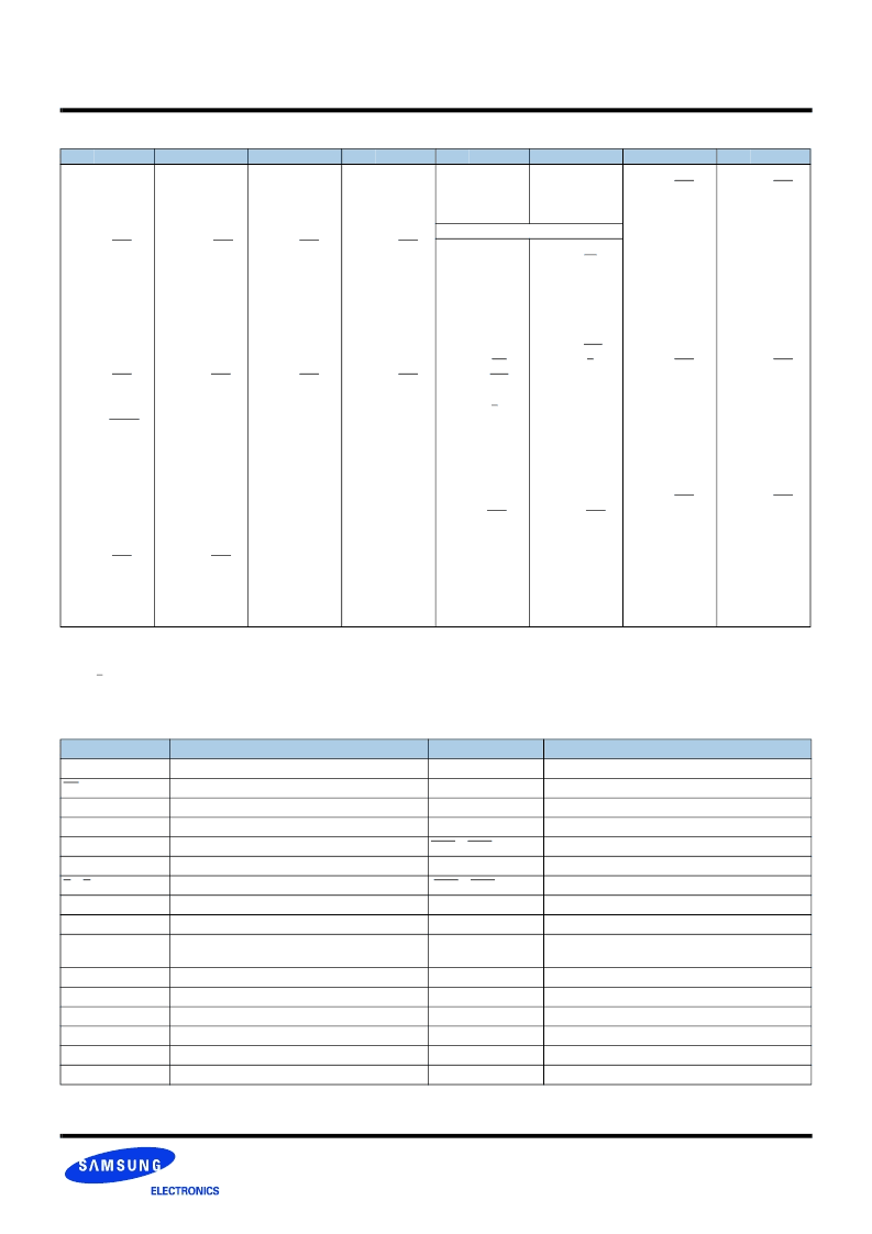
Pin Configurations (Front side/Back side)
Pin
Front
Pin
Back
1
V
REF
121
V
SS
2
V
SS
122
DQ4
3
DQ0
123
DQ5
V
SS
5
V
SS
125
DM0/DQS9
6
DQS0
126
NC/DQS9
V
SS
8
V
SS
128
DQ6
9
DQ2
129
DQ7
V
SS
11
V
SS
131
DQ12
12
DQ8
132
DQ13
V
SS
14
V
SS
134
DM1/DQS10
15
DQS1
135
NC/DQS10
V
SS
17
V
SS
137
RFU
18
RESET
138
RFU
V
SS
20
V
SS
140
DQ14
21
DQ10
141
DQ15
V
SS
23
V
SS
143
DQ20
NC = No Connect, RFU = Reserved for Future Use
1. RESET (Pin 18) is connected to both OE of PLL and Reset of register.
2. The Test pin (Pin 102) is reserved for bus analysis probes and is not connected on normal memory modules (DIMMs)
3. NC/Err_Out ( Pin 55) and NC/Par_In (Pin 68) are for optional function to check address and command parity.
4. CKE1,S1 Pin is used for double side Registered DIMM.
Pin
31
Front
DQ19
V
SS
DQ24
Pin
151
Back
V
SS
DQ28
Pin
61
Front
A4
V
DDQ
A2
V
DD
Pin
181
Back
V
DDQ
A3
Pin
91
Front
V
SS
DQS5
Pin
211
Back
DM5/DQS14
32
152
62
182
92
212
NC/DQS14
V
SS
DQ46
33
153
DQ29
V
SS
63
183
A1
V
DD
93
DQS5
V
SS
DQ42
213
4
DQ1
124
34
DQ25
V
SS
DQS3
154
64
184
94
214
35
155
DM3/DQS12
KEY
95
215
DQ47
V
SS
DQ52
36
156
NC/DQS12
V
SS
DQ30
65
V
SS
V
SS
V
DD
185
CK0
96
DQ43
V
SS
DQ48
216
7
DQS0
127
37
DQS3
V
SS
DQ26
157
66
186
CK0
V
DD
A0
V
DD
BA1
V
DDQ
RAS
97
217
38
158
67
187
98
218
DQ53
V
SS
RFU
39
159
DQ31
V
SS
CB4
68
NC/Par_In
V
DD
A10/AP
188
99
DQ49
V
SS
SA2
219
10
DQ3
130
40
DQ27
V
SS
CB0
160
69
189
100
220
41
161
70
190
101
221
RFU
V
SS
42
162
CB5
V
SS
71
BA0
V
DDQ
WE
191
102
NC(TEST)
V
SS
DQS6
222
13
DQ9
133
43
CB1
V
SS
DQS8
163
72
192
103
223
DM6/DQS15
44
164
DM8/DQS17
73
193
S0
104
224
NC/DQS15
V
SS
DQ54
45
165
NC/DQS17
V
SS
CB6
74
CAS
V
DDQ
S1
4
ODT1
V
DDQ
V
SS
DQ32
194
V
DDQ
ODT0
105
DQS6
V
SS
DQ50
225
16
DQS1
136
46
DQS8
V
SS
CB2
166
75
195
106
226
47
167
76
196
A13
V
DD
V
SS
DQ36
107
227
DQ55
V
SS
DQ60
48
168
CB7
V
SS
V
DDQ
CKE1
4
V
DD
77
197
108
DQ51
V
SS
DQ56
228
19
NC
139
49
CB3
V
SS
V
DDQ
CKE0
V
DD
169
78
198
109
229
50
170
79
199
110
230
DQ61
V
SS
51
171
80
200
DQ37
V
SS
111
DQ57
V
SS
DQS7
231
22
DQ11
142
52
172
81
DQ33
V
SS
201
112
232
DM7/DQS16
53
173
NC
82
202
DM4/DQS13
113
233
NC/DQS16
24
DQ16
144
DQ21
V
SS
54
NC
174
NC
V
DDQ
A12
83
DQS4
203
NC/DQS13
V
SS
DQ38
114
DQS7
V
SS
DQ58
234
V
SS
DQ62
25
DQ17
V
SS
DQS2
145
55
NC/Err_Out
V
DDQ
A11
175
84
DQS4
V
SS
DQ34
204
115
235
26
146
DM2/DQS11
56
176
85
205
116
236
DQ63
V
SS
VDDSPD
27
147
NC/DQS11
V
SS
DQ22
DQ23
57
177
A9
V
DD
A8
A6
86
206
DQ39
V
SS
DQ44
DQ45
V
SS
117
DQ59
V
SS
SDA
SCL
237
28
DQS2
V
SS
DQ18
148
58
A7
V
DD
A5
178
87
DQ35
V
SS
DQ40
DQ41
207
118
238
29
30
149
150
59
60
179
180
88
89
90
208
209
210
119
120
239
240
SA0
SA1
Pin Description
*The VDD and VDDQ pins are tied to the single power-plane on PCB.
Pin Name
Description
Pin Name
Description
CK0
Clock Inputs, positive line
ODT0~ODT1
On die termination
CK0
Clock inputs, negative line
DQ0~DQ63
Data Input/Output
CKE0, CKE1
Clock Enables
CB0~CB7
Data check bits Input/Output
RAS
Row Address Strobe
DQS0~DQS8
Data strobes
CAS
Column Address Strobe
DQS0~DQS8
Data strobes, negative line
WE
Write Enable
DM(0~8),DQS(9~17)
Data Masks / Data strobes (Read)
S0, S1
Chip Selects
DQS9~DQS17
Data strobes (Read), negative line
A0~A9, A11~A13
Address Inputs
RFU
Reserved for Future Use
A10/AP
Address Input/Autoprecharge
NC
No Connect
BA0, BA1
DDR2 SDRAM Bank Address
TEST
Memory bus test tool
(Not Connect and Not Useable on DIMMs)
SCL
Serial Presence Detect (SPD) Clock Input
V
DD
V
DDQ
V
SS
V
REF
V
DDSPD
Core Power
SDA
SPD Data Input/Output
I/O Power
SA0~SA2
SPD address
Ground
Par_In
Parity bit for the Address and Control bus
Input/Output Reference
Err_Out
Parity error found in the Address and Control bus
SPD Power
RESET
Register and PLL control pin
相關(guān)PDF資料 |
PDF描述 |
|---|---|
| M393T5750CZA-CE7 | DDR2 Registered SDRAM MODULE 240pin Registered Module based on 512Mb C-die 72-bit ECC |
| M393T2950CZA-CE6 | DDR2 Registered SDRAM MODULE 240pin Registered Module based on 512Mb C-die 72-bit ECC |
| M393T2950CZA-CE7 | DDR2 Registered SDRAM MODULE 240pin Registered Module based on 512Mb C-die 72-bit ECC |
| M393T2953CZA-CE6 | DDR2 Registered SDRAM MODULE 240pin Registered Module based on 512Mb C-die 72-bit ECC |
| M393T2953CZA-CE7 | DDR2 Registered SDRAM MODULE 240pin Registered Module based on 512Mb C-die 72-bit ECC |
相關(guān)代理商/技術(shù)參數(shù) |
參數(shù)描述 |
|---|---|
| M393T5750CZA-CE600 | 制造商:Samsung Semiconductor 功能描述:512MSDDDRII_MDDR SDRAM MODULX72BOC(LF) - Bulk |
| M393T5750CZA-CE7 | 制造商:SAMSUNG 制造商全稱:Samsung semiconductor 功能描述:DDR2 Registered SDRAM MODULE 240pin Registered Module based on 512Mb C-die 72-bit ECC |
| M393T5750EZA-CE600 | 制造商:Samsung Semiconductor 功能描述:512 DDR SDRAM MODUL X72 BOC(LF) - Trays |
| M393T6450FG0-CC | 制造商:SAMSUNG 制造商全稱:Samsung semiconductor 功能描述:DDR2 Registered SDRAM MODULE 240pin Registered Module based on 256Mb F-die 72-bit ECC |
| M393T6450FG0-CD5/CC | 制造商:SAMSUNG 制造商全稱:Samsung semiconductor 功能描述:DDR2 Registered SDRAM MODULE 240pin Registered Module based on 256Mb F-die 72-bit ECC |
發(fā)布緊急采購,3分鐘左右您將得到回復。