- 您現(xiàn)在的位置:買賣IC網(wǎng) > PDF目錄383298 > M393T5663CZ3 (SAMSUNG SEMICONDUCTOR CO. LTD.) DDR2 Registered SDRAM MODULE PDF資料下載
參數(shù)資料
| 型號: | M393T5663CZ3 |
| 廠商: | SAMSUNG SEMICONDUCTOR CO. LTD. |
| 英文描述: | DDR2 Registered SDRAM MODULE |
| 中文描述: | 注冊的DDR2 SDRAM內(nèi)存模塊 |
| 文件頁數(shù): | 4/26頁 |
| 文件大小: | 618K |
| 代理商: | M393T5663CZ3 |
第1頁第2頁第3頁當(dāng)前第4頁第5頁第6頁第7頁第8頁第9頁第10頁第11頁第12頁第13頁第14頁第15頁第16頁第17頁第18頁第19頁第20頁第21頁第22頁第23頁第24頁第25頁第26頁
Rev. 1.4 November 2007
RDIMM
DDR2 SDRAM
4 of 26
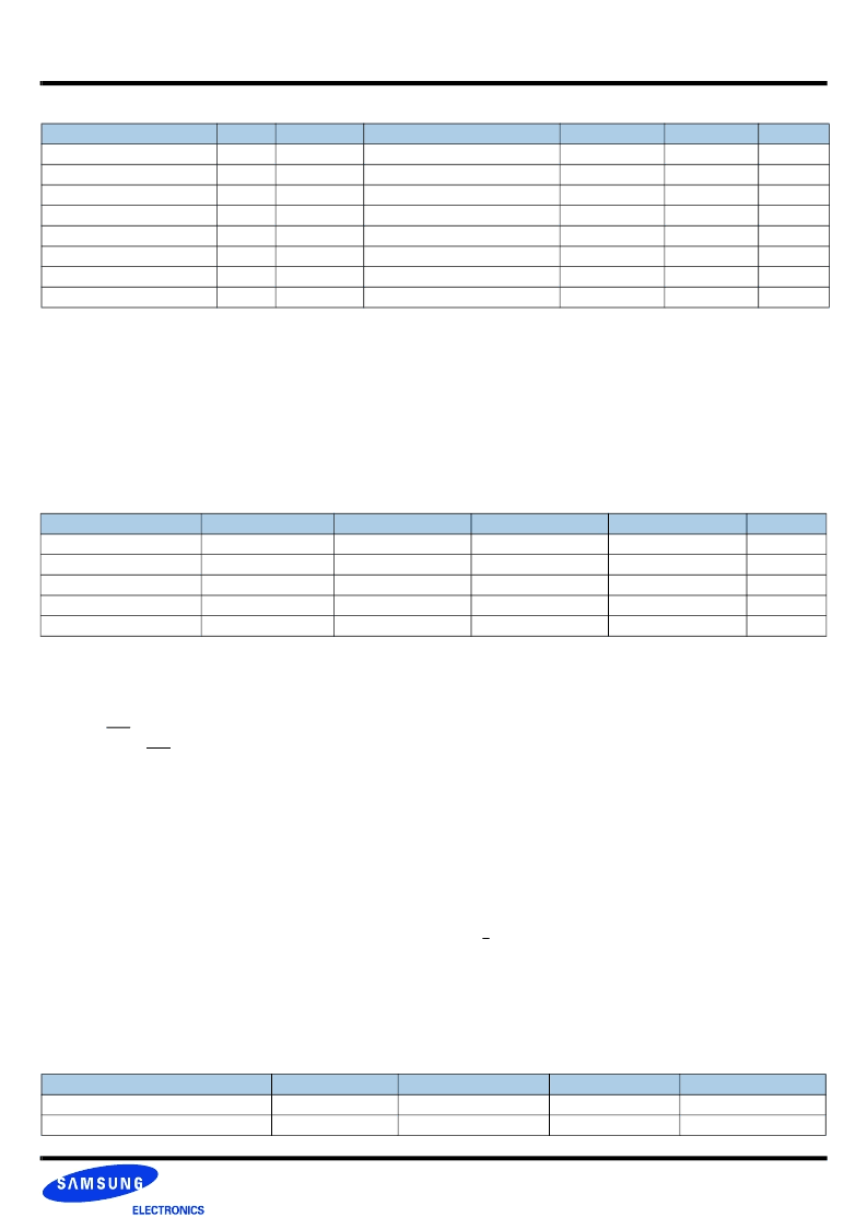
1.0 DDR2 Registered DIMM Ordering Information
Note :
1. “Z” of Part number(11th digit) stand for Lead-free products. and "J" of Part number(11th digit) stand for dual-die package products.
2. “3” of Part number(12th digit) stand for Non-parity Register products. and "A" of Part number(12th digit) stand for Parity Register products.
3. "92" of Part number(3~4th digit) stand for VLP(Very Low Profile) Register products.
Part Number
Density
Organization
Component Composition
Number of Rank
Parity Register
Height
M393T5663CZ3-CD5/CC
2GB
256Mx72
128Mx8(K4T1G084QC)*18EA
2
X
30.00mm
M393T5663CZA-CF7/E6
2GB
256Mx72
128Mx8(K4T1G084QC)*18EA
2
O
30.00mm
M393T5660CZ3-CD5/CC
2GB
256Mx72
256Mx4(K4T1G044QC)*18EA
1
X
30.00mm
M393T5660CZA-CF7/E6
2GB
256Mx72
256Mx4(K4T1G044QC)*18EA
1
O
30.00mm
M393T5160CZ3-CD5/CC
4GB
512Mx72
256Mx4(K4T1G044QC)*36EA
2
X
30.00mm
M393T5160CZA-CF7/E6
4GB
512Mx72
256Mx4(K4T1G044QC)*36EA
2
O
30.00mm
M392T5160CJA-CF7/E6
4GB
512Mx72
DDP512Mx4(K4T2G044QC)*18EA
2
O
18.30mm
M393T1G60CJA-CE6/D5
8GB
1Gx72
DDP512Mx4(K4T1G044QC)*36EA
4
O
30.00mm
Organization
Row Address
Column Address
Bank Address
Auto Precharge
256Mx4(1Gb) based Module
A0-A13
A0-A9, A11
BA0-BA2
A10
128Mx8(1Gb) based Module
A0-A13
A0-A9
BA0-BA2
A10
Performance range
JEDEC standard 1.8V ± 0.1V Power Supply
V
DDQ
= 1.8V ± 0.1V
200 MHz f
CK
for 400Mb/sec/pin, 267MHz f
CK
for 533Mb/sec/pin, 333MHz f
CK
for 667Mb/sec/pin, 400MHz f
CK
for 800Mb/sec/pin
8 Banks
Posted CAS
Programmable CAS Latency: 3, 4, 5, 6
Programmable Additive Latency: 0, 1 , 2 , 3, 4 and 5
Write Latency(WL) = Read Latency(RL) -1
Burst Length: 4 , 8(Interleave/nibble sequential)
Programmable Sequential / Interleave Burst Mode
Bi-directional Differential Data-Strobe (Single-ended data-strobe is an optional feature)
Off-Chip Driver(OCD) Impedance Adjustment
On Die Termination with selectable values(50/75/150 ohms or disable)
PASR(Partial Array Self Refresh)
Average Refresh Period 7.8us at lower than a T
CASE
85
°
C, 3.9us at 85
°
C < T
CASE
< 95
°
C
- support High Temperature Self-Refresh rate enable feature
Serial presence detect with EEPROM
DDR2 SDRAM Package: 60ball FBGA - 128Mx4/64Mx8
All of Lead-free products are compliant for RoHS
Note: For detailed DDR2 SDRAM operation, please refer to Samsung’s Device operation & Timing diagram.
F7(DDR2-800)
E6(DDR2-667)
D5(DDR2-533)
CC(DDR2-400)
Unit
Speed@CL3
-
400
400
400
Mbps
Speed@CL4
533
533
533
400
Mbps
Speed@CL5
667
667
-
-
Mbps
Speed@CL6
800
-
-
-
Mbps
CL-tRCD-tRP
6-6-6
5-5-5
4-4-4
3-3-3
CK
2.0 Features
3.0 Address Configuration
相關(guān)PDF資料 |
PDF描述 |
|---|---|
| M393T5663CZ3-CD5 | DDR2 Registered SDRAM MODULE |
| M393T5663CZA-CF7 | DDR2 Registered SDRAM MODULE |
| M393T2953CZA-CCC | DDR2 Registered SDRAM MODULE 240pin Registered Module based on 512Mb C-die 72-bit ECC |
| M393T2953CZ3-CCC | 40 characters x 2 Lines, 5x7 Dot Matric Character and Cursor |
| M393T2950CZ3-CCC | 40 characters x 2 Lines, 5x7 Dot Matric Character and Cursor |
相關(guān)代理商/技術(shù)參數(shù) |
參數(shù)描述 |
|---|---|
| M393T5663CZ3-CD5 | 制造商:SAMSUNG 制造商全稱:Samsung semiconductor 功能描述:DDR2 Registered SDRAM MODULE |
| M393T5663CZA-CF7 | 制造商:SAMSUNG 制造商全稱:Samsung semiconductor 功能描述:DDR2 Registered SDRAM MODULE |
| M393T5663QZ3 | 制造商:SAMSUNG 制造商全稱:Samsung semiconductor 功能描述:DDR2 SDRAM Memory |
| M393T5663QZHA | 制造商:SAMSUNG 制造商全稱:Samsung semiconductor 功能描述:DDR2 SDRAM Memory |
| M393T5750BS0-CD5/CC | 制造商:SAMSUNG 制造商全稱:Samsung semiconductor 功能描述:DDR2 Registered SDRAM MODULE 240pin Registered Module based on 512Mb B-die 72-bit ECC |
發(fā)布緊急采購,3分鐘左右您將得到回復(fù)。