- 您現(xiàn)在的位置:買賣IC網(wǎng) > PDF目錄224144 > M38B52E6XXXFP (Renesas Technology Corp.) SINGLE-CHIP 8-BIT CMOS MICROCOMPUTER PDF資料下載
參數(shù)資料
| 型號: | M38B52E6XXXFP |
| 廠商: | Renesas Technology Corp. |
| 英文描述: | SINGLE-CHIP 8-BIT CMOS MICROCOMPUTER |
| 中文描述: | 單芯片8位CMOS微機 |
| 文件頁數(shù): | 46/70頁 |
| 文件大小: | 864K |
| 代理商: | M38B52E6XXXFP |
第1頁第2頁第3頁第4頁第5頁第6頁第7頁第8頁第9頁第10頁第11頁第12頁第13頁第14頁第15頁第16頁第17頁第18頁第19頁第20頁第21頁第22頁第23頁第24頁第25頁第26頁第27頁第28頁第29頁第30頁第31頁第32頁第33頁第34頁第35頁第36頁第37頁第38頁第39頁第40頁第41頁第42頁第43頁第44頁第45頁當前第46頁第47頁第48頁第49頁第50頁第51頁第52頁第53頁第54頁第55頁第56頁第57頁第58頁第59頁第60頁第61頁第62頁第63頁第64頁第65頁第66頁第67頁第68頁第69頁第70頁
MITSUBISHI MICROCOMPUTERS
38B5 Group
SINGLE-CHIP 8-BIT CMOS MICROCOMPUTER
49
PRELIMINAR
Y
Notice:
This
is not
a final
specification.
Some
parametric
lim
its are
subject
to change.
1. Data setup
The PWM output pin also function as port P87. Set port P87 to be the
PWM output pin by setting bit 0 of the PWM control register (address
002616) to “1.” The high-order 8 bits of output data are set in the
high-order PWM register PWMH (address 001416) and the low-order
6 bits are set in the low-order PWM register PWML (address 001516).
2. PWM operation
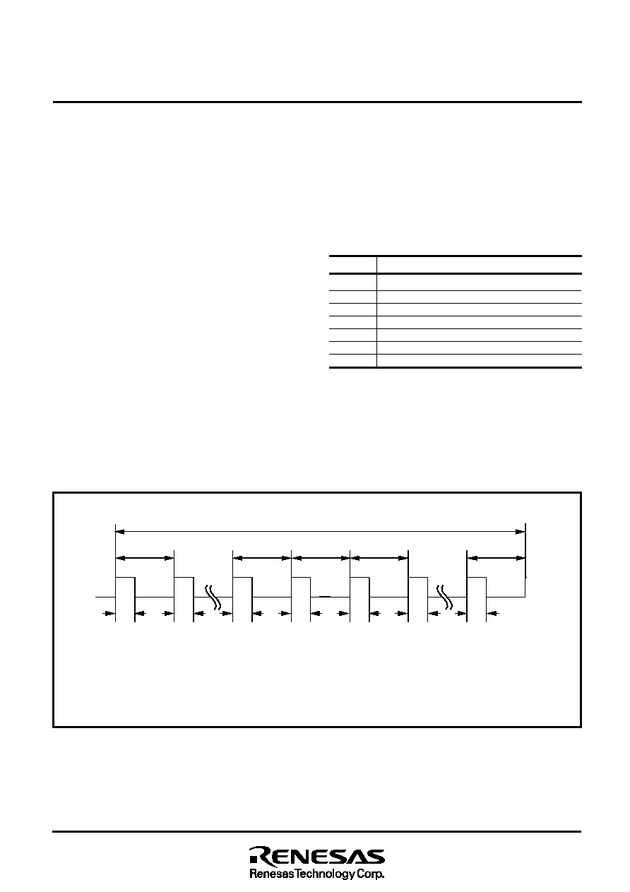
The timing of the 14-bit PWM function is shown in Figure 56.
The 14-bit PWM data is divided into the low-order 6 bits and the
high-order 8 bits in the PWM latch.
The high-order 8 bits of data determine how long an “H” level signal
is output during each sub-period. There are 64 sub-periods in each
period, and each sub-period t is 256
τ (= 64 s) long. The signal’s
“H” has a length equal to N times
τ, and its minimum resolution = 250
ns.
The last bit of the sub-period becomes the ADD bit which is specified
either “H” or “L,” by the contents of PWML. As shown in Table 8, the
ADD bit is decided either “H” or “L.”
That is, only in the sub-period tm shown in Table 8 in the PWM cycle
period T = 64t, the “H” duration is lengthened during the minimum
resolution width
τ period in comparison with the other period.
For example, if the high-order eight bits of the 14-bit data are “0316”
and the low-order six bits are “0516,” the length of the “H” level output
in sub-periods t8, t24, t32, t40 and t56 is 4
τ, and its length 3 τ in all other
sub-periods.
Time at the “H” level of each sub-period almost becomes equal be-
cause the time becomes length set in the high-order 8 bits or be-
comes the value plus
τ, and this sub-period t (= 64 s, approximate
15.6 kHz) becomes cycle period approximately.
3. Transfer from register to latch
Data written to the PWML register is transferred to the PWM latch
once in each PWM period (every 4096 s), and data written to the
PWMH register is transferred to the PWM latch once in each sub-
period (every 64 s). When the PWML register is read, the contents
of the latch are read. However, bit 7 of the PWML register indicates
whether the transfer to the PWM latch is completed; the transfer is
completed when bit 7 is “0.”
Table 8 Relationship between Low-order 6-bit Data and Setting
Period of ADD Bit
Low-order
6-bit data
Sub-periods tm lengthened (m = 0 to 63)
0 0 0 0 0 0
None
0 0 0 0 0 1
m = 32
0 0 0 0 1 0
m = 16, 48
0 0 0 1 0 0
m = 8, 24, 40, 56
0 0 1 0 0 0
m = 4, 12, 20, 28, 36, 44, 52, 60
0 1 0 0 0 0
m = 2, 6, 10, 14, 18, 22, 26, 30, 34, 38, 42, 46, 50, 54, 58, 62
1 0 0 0 0 0
m = 1, 3, 5, 7, .................................................., 57, 59, 61, 63
LSB
Fig. 54 PWM Timing
15.75
s
64
s
64
s
64
s
64
s
64
s
m = 0
m = 7
m = 8
m = 9
m = 63
16.0
s
15.75
s
15.75
s
15.75
s
15.75
s
15.75
s
Pulse width modulation register H: 00111111
Pulse width modulation register L: 000101
Sub-periods where “H” pulse width is 16.0
s: m = 8, 24, 32, 40, 56
Sub-periods where “H” pulse width is 15.75
s: m = all other values
4096
s
相關PDF資料 |
PDF描述 |
|---|---|
| M38B52E6XXXFS | SINGLE-CHIP 8-BIT CMOS MICROCOMPUTER |
| M39012/04-0001 | PANEL MOUNT, CABLE TERMINATED, FEMALE, N CONNECTOR, SOLDER, RECEPTACLE |
| M39012/04-0002 | PANEL MOUNT, FEMALE, N CONNECTOR, SOLDER, RECEPTACLE |
| M39012/13-0001 | PANEL MOUNT, FEMALE, BNC CONNECTOR, RECEPTACLE |
| M39012/16-0502 | CABLE TERMINATED, MALE, BNC CONNECTOR, CRIMP, PLUG |
相關代理商/技術參數(shù) |
參數(shù)描述 |
|---|---|
| M38B52E6XXXFS | 制造商:RENESAS 制造商全稱:Renesas Technology Corp 功能描述:SINGLE-CHIP 8-BIT CMOS MICROCOMPUTER |
| M38B52E7XXXFP | 制造商:RENESAS 制造商全稱:Renesas Technology Corp 功能描述:SINGLE-CHIP 8-BIT CMOS MICROCOMPUTER |
| M38B52E7XXXFS | 制造商:RENESAS 制造商全稱:Renesas Technology Corp 功能描述:SINGLE-CHIP 8-BIT CMOS MICROCOMPUTER |
| M38B52E8XXXFP | 制造商:RENESAS 制造商全稱:Renesas Technology Corp 功能描述:SINGLE-CHIP 8-BIT CMOS MICROCOMPUTER |
| M38B52E8XXXFS | 制造商:RENESAS 制造商全稱:Renesas Technology Corp 功能描述:SINGLE-CHIP 8-BIT CMOS MICROCOMPUTER |
發(fā)布緊急采購,3分鐘左右您將得到回復。