- 您現(xiàn)在的位置:買賣IC網(wǎng) > PDF目錄370955 > M38867M8A-A06HP (Mitsubishi Electric Corporation) SINGLE-CHIP 8-BIT CMOS MICROCOMPUTER PDF資料下載
參數(shù)資料
| 型號: | M38867M8A-A06HP |
| 廠商: | Mitsubishi Electric Corporation |
| 英文描述: | SINGLE-CHIP 8-BIT CMOS MICROCOMPUTER |
| 中文描述: | 單芯片8位CMOS微機 |
| 文件頁數(shù): | 78/110頁 |
| 文件大小: | 1601K |
| 代理商: | M38867M8A-A06HP |
第1頁第2頁第3頁第4頁第5頁第6頁第7頁第8頁第9頁第10頁第11頁第12頁第13頁第14頁第15頁第16頁第17頁第18頁第19頁第20頁第21頁第22頁第23頁第24頁第25頁第26頁第27頁第28頁第29頁第30頁第31頁第32頁第33頁第34頁第35頁第36頁第37頁第38頁第39頁第40頁第41頁第42頁第43頁第44頁第45頁第46頁第47頁第48頁第49頁第50頁第51頁第52頁第53頁第54頁第55頁第56頁第57頁第58頁第59頁第60頁第61頁第62頁第63頁第64頁第65頁第66頁第67頁第68頁第69頁第70頁第71頁第72頁第73頁第74頁第75頁第76頁第77頁當(dāng)前第78頁第79頁第80頁第81頁第82頁第83頁第84頁第85頁第86頁第87頁第88頁第89頁第90頁第91頁第92頁第93頁第94頁第95頁第96頁第97頁第98頁第99頁第100頁第101頁第102頁第103頁第104頁第105頁第106頁第107頁第108頁第109頁第110頁

78
3886 Group
SINGLE-CHIP 8-BIT CMOS MICROCOMPUTER
MITSUBISHI MICROCOMPUTERS
G
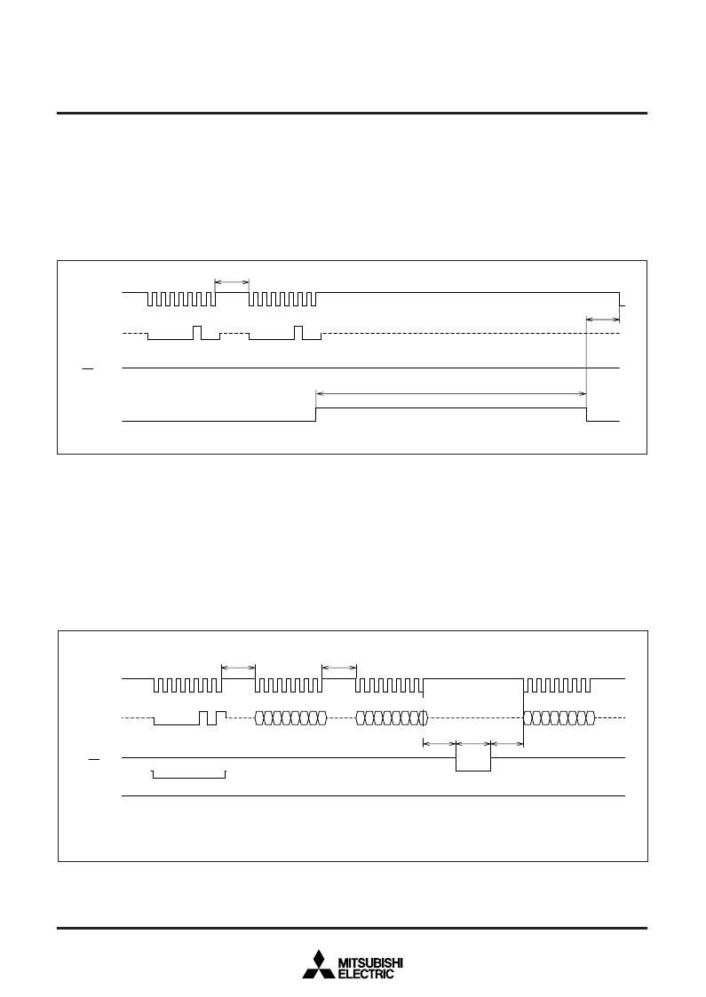
Erase command
Input command code 20
16
in the first transfer and command code
20
16
again in the second transfer. When this is done, the
M38869FFAHP/GP executes an erase command. Erase is initi-
ated at the last rising edge of the serial clock. The BUSY pin is
driven high during the erase operation. Erase is completed within
9.5 ms as measured by the internal timer, and the BUSY pin is
pulled low. Note that data 00
16
must be written to all memory loca-
tions before executing the erase command.
Note:
A erase operation is not completed by executing the erase
command once. Always be sure to execute a erase verify
command after executing the erase command. When the fail-
ure is found in the verification, the user must repeatedly ex-
ecute the erase command until the pass in the verification.
Refer to Figure 71 for the erase flowchart.
Fig. 76 Timings at erasing
G
Erase verify command
The user must verify the contents of all addresses after complet-
ing the erase command. Input command code A0
16
in the first
transfer. Proceed and input the low-order 8 bits and the high-order
8 bits of the address and pull the OE pin low. When this is done,
the M38869FFAHP/GP reads out the contents of the specified ad-
dress, and then latchs it into the internal data latch. When the OE
pin is released back high and serial clock is input to the SCLK pin,
the verify data that has been latched into the data latch is serially
output from the SDA pin.
Note:
If any memory location where the contents have not been
erased is found in the erase verify operation, execute the op-
eration of “erase
→
erase verify” over again. In this case,
however, the user does not need to write data 00
16
to memory
locations before erasing.
Fig. 77 Timings during erase verify
tw
E
SCLK
BUSY
OE
SDA
t
CH
t
EC
0 0 0 0 0 1 0 0
Command code input (20
16
) Command code input (20
16
)
0 0 0 0 0 1 0 0
Erase
“H”
“L”
SCLK
BUSY
OE
SDA
t
CH
A
0
A
7
A
8
A
15
D
0
D
7
t
CH
t
CREV
Command code input (A0
16
) Verify address input (L)
Verify address input (H)
Verify data output
t
WR
Verify read
t
RC
Note :
When outputting the verify data, the SDA pin is switched for output at the first falling edge of SCLK. The SDA pin is placed
in the floating state during the period of th
(C-E)
after the last rising edge of SCLK (at the 8th bit).
0 0 0 0 0 1 0 1
相關(guān)PDF資料 |
PDF描述 |
|---|---|
| M38867M8A-A07HP | connectors |
| M38867M8A-A11HP | SINGLE-CHIP 8-BIT CMOS MICROCOMPUTER |
| M38869FFAHP | SINGLE-CHIP 8-BIT CMOS MICROCOMPUTER |
| M38869M8A-XXXGP | SINGLE-CHIP 8-BIT CMOS MICROCOMPUTER |
| M38869M8A-XXXHP | SINGLE-CHIP 8-BIT CMOS MICROCOMPUTER |
相關(guān)代理商/技術(shù)參數(shù) |
參數(shù)描述 |
|---|---|
| M38867M8A-A07HP | 制造商:MITSUBISHI 制造商全稱:Mitsubishi Electric Semiconductor 功能描述:SINGLE-CHIP 8-BIT CMOS MICROCOMPUTER |
| M38867M8A-A11HP | 制造商:MITSUBISHI 制造商全稱:Mitsubishi Electric Semiconductor 功能描述:SINGLE-CHIP 8-BIT CMOS MICROCOMPUTER |
| M38867M8A-XXXHP | 制造商:MITSUBISHI 制造商全稱:Mitsubishi Electric Semiconductor 功能描述:SINGLE-CHIP 8-BIT CMOS MICROCOMPUTER |
| M38867M8-XXXHP | 制造商:RENESAS 制造商全稱:Renesas Technology Corp 功能描述:SINGLE-CHIP 8-BIT CMOS MICROCOMPUTER |
| M38867M9-XXXHP | 制造商:RENESAS 制造商全稱:Renesas Technology Corp 功能描述:SINGLE-CHIP 8-BIT CMOS MICROCOMPUTER |
發(fā)布緊急采購,3分鐘左右您將得到回復(fù)。