- 您現(xiàn)在的位置:買賣IC網(wǎng) > PDF目錄45043 > M38199MF-XXXFP 8-BIT, MROM, MICROCONTROLLER, PQFP100 PDF資料下載
參數(shù)資料
| 型號(hào): | M38199MF-XXXFP |
| 元件分類: | 微控制器/微處理器 |
| 英文描述: | 8-BIT, MROM, MICROCONTROLLER, PQFP100 |
| 封裝: | 14 X 20 MM, PLASTIC, QFP-100 |
| 文件頁(yè)數(shù): | 197/217頁(yè) |
| 文件大小: | 2564K |
| 代理商: | M38199MF-XXXFP |
第1頁(yè)第2頁(yè)第3頁(yè)第4頁(yè)第5頁(yè)第6頁(yè)第7頁(yè)第8頁(yè)第9頁(yè)第10頁(yè)第11頁(yè)第12頁(yè)第13頁(yè)第14頁(yè)第15頁(yè)第16頁(yè)第17頁(yè)第18頁(yè)第19頁(yè)第20頁(yè)第21頁(yè)第22頁(yè)第23頁(yè)第24頁(yè)第25頁(yè)第26頁(yè)第27頁(yè)第28頁(yè)第29頁(yè)第30頁(yè)第31頁(yè)第32頁(yè)第33頁(yè)第34頁(yè)第35頁(yè)第36頁(yè)第37頁(yè)第38頁(yè)第39頁(yè)第40頁(yè)第41頁(yè)第42頁(yè)第43頁(yè)第44頁(yè)第45頁(yè)第46頁(yè)第47頁(yè)第48頁(yè)第49頁(yè)第50頁(yè)第51頁(yè)第52頁(yè)第53頁(yè)第54頁(yè)第55頁(yè)第56頁(yè)第57頁(yè)第58頁(yè)第59頁(yè)第60頁(yè)第61頁(yè)第62頁(yè)第63頁(yè)第64頁(yè)第65頁(yè)第66頁(yè)第67頁(yè)第68頁(yè)第69頁(yè)第70頁(yè)第71頁(yè)第72頁(yè)第73頁(yè)第74頁(yè)第75頁(yè)第76頁(yè)第77頁(yè)第78頁(yè)第79頁(yè)第80頁(yè)第81頁(yè)第82頁(yè)第83頁(yè)第84頁(yè)第85頁(yè)第86頁(yè)第87頁(yè)第88頁(yè)第89頁(yè)第90頁(yè)第91頁(yè)第92頁(yè)第93頁(yè)第94頁(yè)第95頁(yè)第96頁(yè)第97頁(yè)第98頁(yè)第99頁(yè)第100頁(yè)第101頁(yè)第102頁(yè)第103頁(yè)第104頁(yè)第105頁(yè)第106頁(yè)第107頁(yè)第108頁(yè)第109頁(yè)第110頁(yè)第111頁(yè)第112頁(yè)第113頁(yè)第114頁(yè)第115頁(yè)第116頁(yè)第117頁(yè)第118頁(yè)第119頁(yè)第120頁(yè)第121頁(yè)第122頁(yè)第123頁(yè)第124頁(yè)第125頁(yè)第126頁(yè)第127頁(yè)第128頁(yè)第129頁(yè)第130頁(yè)第131頁(yè)第132頁(yè)第133頁(yè)第134頁(yè)第135頁(yè)第136頁(yè)第137頁(yè)第138頁(yè)第139頁(yè)第140頁(yè)第141頁(yè)第142頁(yè)第143頁(yè)第144頁(yè)第145頁(yè)第146頁(yè)第147頁(yè)第148頁(yè)第149頁(yè)第150頁(yè)第151頁(yè)第152頁(yè)第153頁(yè)第154頁(yè)第155頁(yè)第156頁(yè)第157頁(yè)第158頁(yè)第159頁(yè)第160頁(yè)第161頁(yè)第162頁(yè)第163頁(yè)第164頁(yè)第165頁(yè)第166頁(yè)第167頁(yè)第168頁(yè)第169頁(yè)第170頁(yè)第171頁(yè)第172頁(yè)第173頁(yè)第174頁(yè)第175頁(yè)第176頁(yè)第177頁(yè)第178頁(yè)第179頁(yè)第180頁(yè)第181頁(yè)第182頁(yè)第183頁(yè)第184頁(yè)第185頁(yè)第186頁(yè)第187頁(yè)第188頁(yè)第189頁(yè)第190頁(yè)第191頁(yè)第192頁(yè)第193頁(yè)第194頁(yè)第195頁(yè)第196頁(yè)當(dāng)前第197頁(yè)第198頁(yè)第199頁(yè)第200頁(yè)第201頁(yè)第202頁(yè)第203頁(yè)第204頁(yè)第205頁(yè)第206頁(yè)第207頁(yè)第208頁(yè)第209頁(yè)第210頁(yè)第211頁(yè)第212頁(yè)第213頁(yè)第214頁(yè)第215頁(yè)第216頁(yè)第217頁(yè)
67
3819 Group
SINGLE-CHIP 8-BIT CMOS MICROCOMPUTER
MITSUBISHI MICROCOMPUTERS
A-D converter
A-D conversion is started by setting A-D conversion completion bit to “0”. During A-D conversion, internal operations
are performed as follows.
1. After the start of A-D conversion, A-D conversion register goes to “0016.”
2. The highest-order bit of A-D conversion register is set to “1”, and the comparison voltage Vref is input to the
comparator. Then, Vref is compared with analog input voltage VIN.
3. As a result of comparison, when Vref < VIN, the highest-order bit of A-D conversion register becomes “1.” When
Vref > VIN, the highest-order bit becomes “0.”
By repeating the above operations up to the lowest-order bit of the A-D conversion register, an analog value converts
into a digital value.
A-D conversion completes at 50 clock cycles (11.9
s at f(XIN) = 8.4 MHz) after it is started, and the result of the
conversion is stored into the A-D conversion register.
Concurrently with the completion of A-D conversion, A-D conversion interrupt request occurs, so that the A-D
conversion interrupt request bit is set to “1”.
Relative formula for a reference voltage VREF of A-D converter and Vref
When n = 0
Vref = 0
When n = 1 to 255
Vref =
! (n–0.5)
n : the value of A-D converter (decimal numeral)
VREF
256
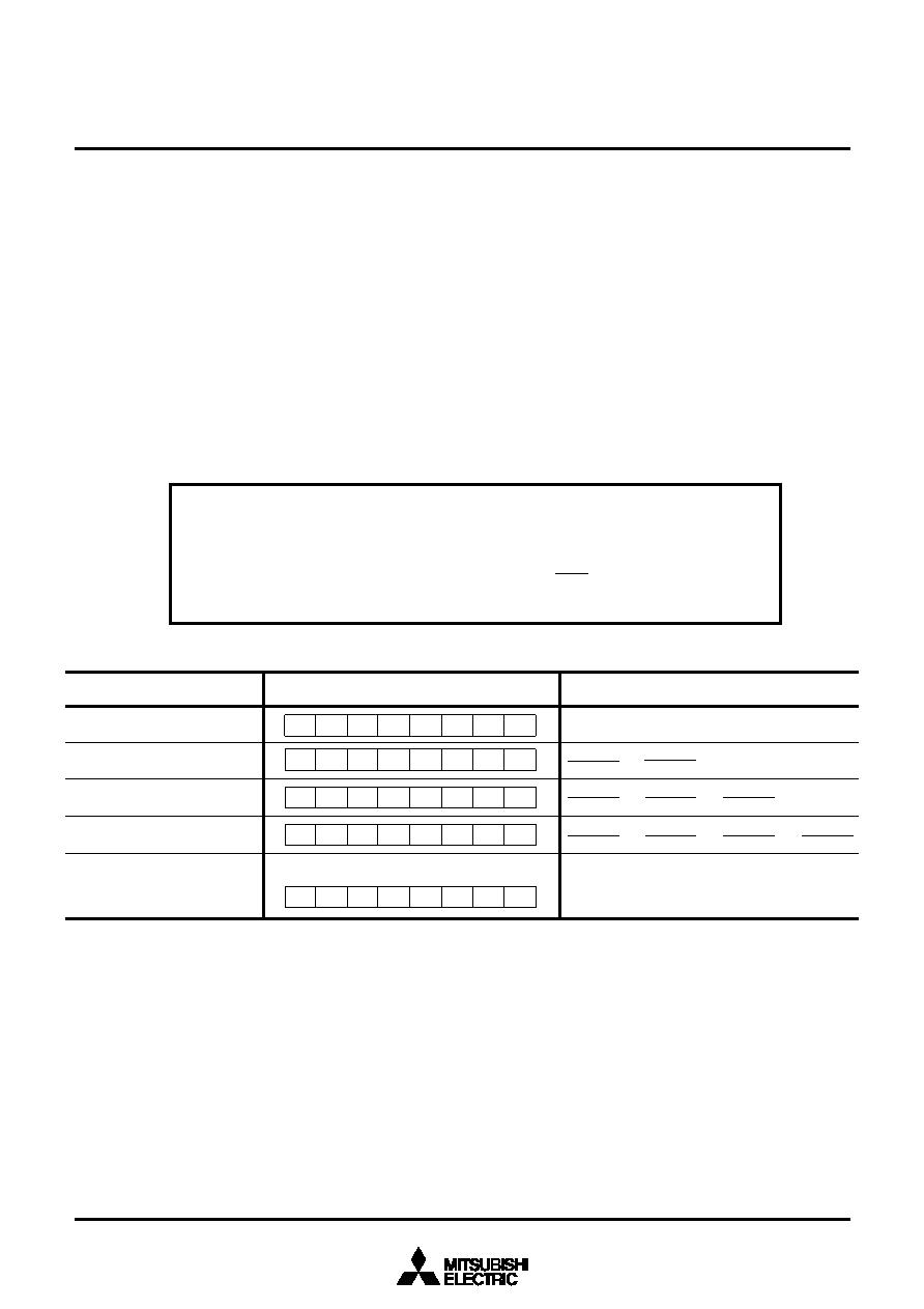
Table 6. Change of A-D conversion register during A-D conversion
At start of conversion
First comparison
Second comparison
Third comparison
After completion of eighth
comparison
Value of comparison voltage (Vref)
*1 : A result of the first comparison
*3 : A result of the third comparison
*5 : A result of the fifth comparison
*7 : A result of the seventh comparison
*2 : A result of the second comparison
*4 : A result of the fourth comparison
*6 : A result of the sixth comparison
*8 : A result of the eighth comparison
0
2
VREF
512
VREF
–
2
VREF
4
VREF
±
512
VREF
–
2
VREF
4
VREF
±
8
VREF
±
512
VREF
–
A result of A-D conversion
00
0
Change of A-D conversion register
1
0
0000
0
*1
1
0
0000
0
*1
*2
1
0000
0
*1
*2
*3
*4
*5
*6
*7
*8
相關(guān)PDF資料 |
PDF描述 |
|---|---|
| M38203E4-XXXHP | 8-BIT, OTPROM, 8 MHz, MICROCONTROLLER, PQFP80 |
| M38203M4-XXXHP | 8-BIT, MROM, 8 MHz, MICROCONTROLLER, PQFP80 |
| M38207M8-XXXFP | 8-BIT, MROM, 8 MHz, MICROCONTROLLER, PQFP80 |
| M38207E8-XXXFP | 8-BIT, OTPROM, 8 MHz, MICROCONTROLLER, PQFP80 |
| M38207E8-XXXHP | 8-BIT, OTPROM, 8 MHz, MICROCONTROLLER, PQFP80 |
相關(guān)代理商/技術(shù)參數(shù) |
參數(shù)描述 |
|---|---|
| M381A1G43BB0-CQB | 制造商:Samsung SDI 功能描述: |
| M381A1G73BB0-CQB | 制造商:Samsung SDI 功能描述: |
| M381A5173BB0-CQB | 制造商:Samsung SDI 功能描述: |
| M381L2923CUM-CB300 | 制造商:Samsung Semiconductor 功能描述:512MSDDDR_MDDR SDRAM MODULX72TSOP2-400(LF) - Bulk |
| M381L6423ETM-CA200 | 制造商:Samsung Semiconductor 功能描述:256 DDR SDRAM MODUL X72 TSOP2-400 - Trays |
發(fā)布緊急采購(gòu),3分鐘左右您將得到回復(fù)。