- 您現(xiàn)在的位置:買賣IC網(wǎng) > PDF目錄359693 > M38038FB-XXXSP (Renesas Technology Corp.) SINGLE-CHIP 8-BIT CMOS MICROCOMPUTER PDF資料下載
參數(shù)資料
| 型號: | M38038FB-XXXSP |
| 廠商: | Renesas Technology Corp. |
| 英文描述: | SINGLE-CHIP 8-BIT CMOS MICROCOMPUTER |
| 中文描述: | 單芯片8位CMOS微機(jī) |
| 文件頁數(shù): | 33/119頁 |
| 文件大小: | 1575K |
| 代理商: | M38038FB-XXXSP |
第1頁第2頁第3頁第4頁第5頁第6頁第7頁第8頁第9頁第10頁第11頁第12頁第13頁第14頁第15頁第16頁第17頁第18頁第19頁第20頁第21頁第22頁第23頁第24頁第25頁第26頁第27頁第28頁第29頁第30頁第31頁第32頁當(dāng)前第33頁第34頁第35頁第36頁第37頁第38頁第39頁第40頁第41頁第42頁第43頁第44頁第45頁第46頁第47頁第48頁第49頁第50頁第51頁第52頁第53頁第54頁第55頁第56頁第57頁第58頁第59頁第60頁第61頁第62頁第63頁第64頁第65頁第66頁第67頁第68頁第69頁第70頁第71頁第72頁第73頁第74頁第75頁第76頁第77頁第78頁第79頁第80頁第81頁第82頁第83頁第84頁第85頁第86頁第87頁第88頁第89頁第90頁第91頁第92頁第93頁第94頁第95頁第96頁第97頁第98頁第99頁第100頁第101頁第102頁第103頁第104頁第105頁第106頁第107頁第108頁第109頁第110頁第111頁第112頁第113頁第114頁第115頁第116頁第117頁第118頁第119頁
Rev.1.00
REJ03B0212-0100
Apr 2, 2007
Page 33 of 117
3803 Group (Spec.L)
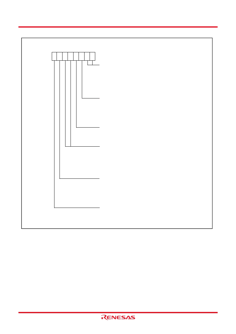
Fig 26. Structure of timer XY mode register
b7
Timer XY mode register
(TM : address 0023
16
)
Timer X operating mode bits
b1 b0
0 0: Timer mode
0 1: Pulse output mode
1 0: Event counter mode
1 1: Pulse width measurement mode
CNTR
0
active edge switch bit
0: Interrupt at falling edge
Count at rising edge in event counter mode
1: Interrupt at rising edge
Count at falling edge in event counter mode
Timer X count stop bit
0: Count start
1: Count stop
Timer Y operating mode bits
b5 b4
0 0: Timer mode
0 1: Pulse output mode
1 0: Event counter mode
1 1: Pulse width measurement mode
CNTR
1
active edge switch bit
0: Interrupt at falling edge
Count at rising edge in event counter mode
1: Interrupt at rising edge
Count at falling edge in event counter mode
Timer Y count stop bit
0: Count start
1: Count stop
b0
發(fā)布緊急采購,3分鐘左右您將得到回復(fù)。