- 您現(xiàn)在的位置:買賣IC網(wǎng) > PDF目錄201874 > M37477M8-XXXSP 8-BIT, MROM, MICROCONTROLLER, PDIP32 PDF資料下載
參數(shù)資料
| 型號: | M37477M8-XXXSP |
| 元件分類: | 微控制器/微處理器 |
| 英文描述: | 8-BIT, MROM, MICROCONTROLLER, PDIP32 |
| 封裝: | 0.400 INCH, 1.78 MM PITCH, SHRINK, PLASTIC, DIP-32 |
| 文件頁數(shù): | 122/353頁 |
| 文件大?。?/td> | 3956K |
| 代理商: | M37477M8-XXXSP |
第1頁第2頁第3頁第4頁第5頁第6頁第7頁第8頁第9頁第10頁第11頁第12頁第13頁第14頁第15頁第16頁第17頁第18頁第19頁第20頁第21頁第22頁第23頁第24頁第25頁第26頁第27頁第28頁第29頁第30頁第31頁第32頁第33頁第34頁第35頁第36頁第37頁第38頁第39頁第40頁第41頁第42頁第43頁第44頁第45頁第46頁第47頁第48頁第49頁第50頁第51頁第52頁第53頁第54頁第55頁第56頁第57頁第58頁第59頁第60頁第61頁第62頁第63頁第64頁第65頁第66頁第67頁第68頁第69頁第70頁第71頁第72頁第73頁第74頁第75頁第76頁第77頁第78頁第79頁第80頁第81頁第82頁第83頁第84頁第85頁第86頁第87頁第88頁第89頁第90頁第91頁第92頁第93頁第94頁第95頁第96頁第97頁第98頁第99頁第100頁第101頁第102頁第103頁第104頁第105頁第106頁第107頁第108頁第109頁第110頁第111頁第112頁第113頁第114頁第115頁第116頁第117頁第118頁第119頁第120頁第121頁當(dāng)前第122頁第123頁第124頁第125頁第126頁第127頁第128頁第129頁第130頁第131頁第132頁第133頁第134頁第135頁第136頁第137頁第138頁第139頁第140頁第141頁第142頁第143頁第144頁第145頁第146頁第147頁第148頁第149頁第150頁第151頁第152頁第153頁第154頁第155頁第156頁第157頁第158頁第159頁第160頁第161頁第162頁第163頁第164頁第165頁第166頁第167頁第168頁第169頁第170頁第171頁第172頁第173頁第174頁第175頁第176頁第177頁第178頁第179頁第180頁第181頁第182頁第183頁第184頁第185頁第186頁第187頁第188頁第189頁第190頁第191頁第192頁第193頁第194頁第195頁第196頁第197頁第198頁第199頁第200頁第201頁第202頁第203頁第204頁第205頁第206頁第207頁第208頁第209頁第210頁第211頁第212頁第213頁第214頁第215頁第216頁第217頁第218頁第219頁第220頁第221頁第222頁第223頁第224頁第225頁第226頁第227頁第228頁第229頁第230頁第231頁第232頁第233頁第234頁第235頁第236頁第237頁第238頁第239頁第240頁第241頁第242頁第243頁第244頁第245頁第246頁第247頁第248頁第249頁第250頁第251頁第252頁第253頁第254頁第255頁第256頁第257頁第258頁第259頁第260頁第261頁第262頁第263頁第264頁第265頁第266頁第267頁第268頁第269頁第270頁第271頁第272頁第273頁第274頁第275頁第276頁第277頁第278頁第279頁第280頁第281頁第282頁第283頁第284頁第285頁第286頁第287頁第288頁第289頁第290頁第291頁第292頁第293頁第294頁第295頁第296頁第297頁第298頁第299頁第300頁第301頁第302頁第303頁第304頁第305頁第306頁第307頁第308頁第309頁第310頁第311頁第312頁第313頁第314頁第315頁第316頁第317頁第318頁第319頁第320頁第321頁第322頁第323頁第324頁第325頁第326頁第327頁第328頁第329頁第330頁第331頁第332頁第333頁第334頁第335頁第336頁第337頁第338頁第339頁第340頁第341頁第342頁第343頁第344頁第345頁第346頁第347頁第348頁第349頁第350頁第351頁第352頁第353頁
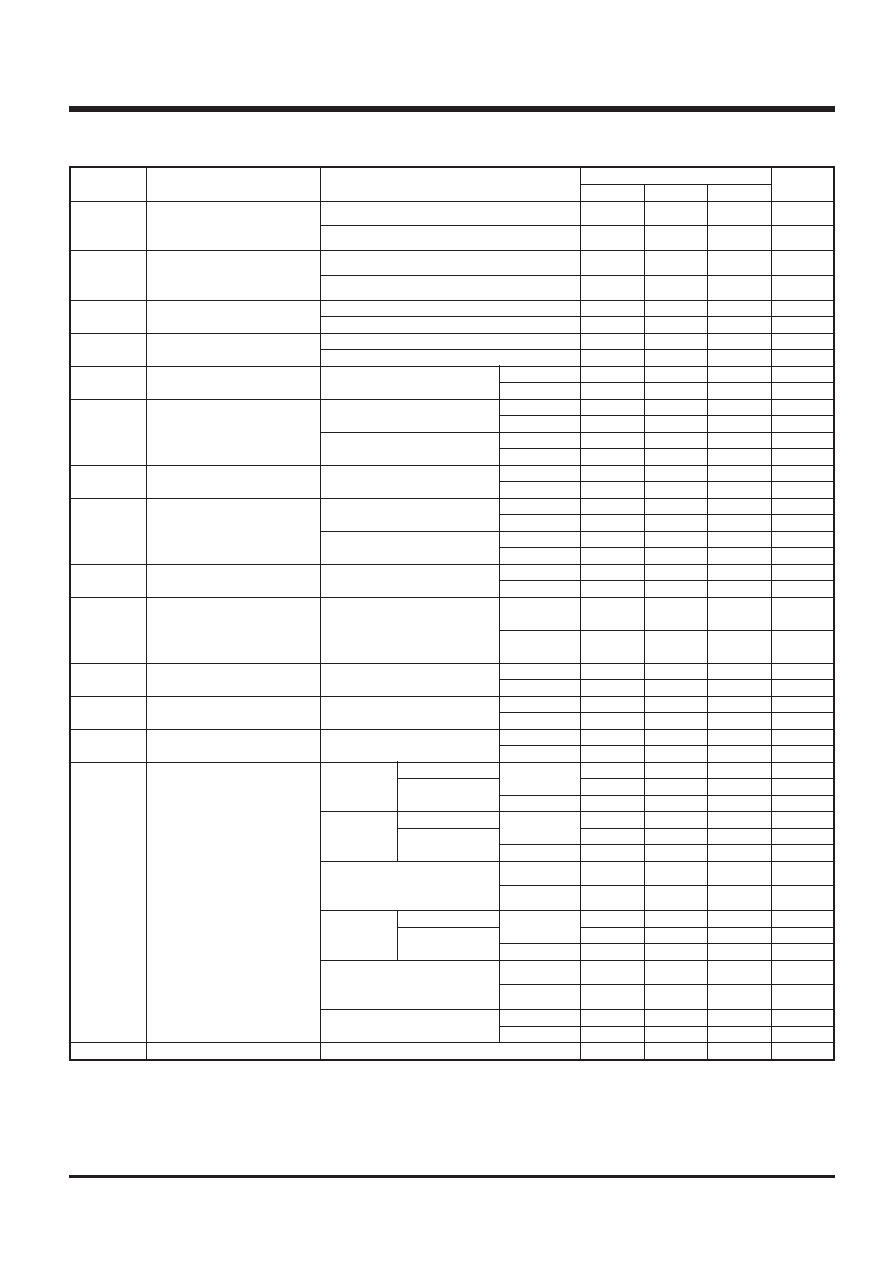
1-192
HARDWARE
1.20 Electrical characteristics
7470/7471/7477/7478 GROUP USER’S MANUAL
Table 1.20.7 Electrical characteristics (7471 group)
(VCC = 2.7 V to 5.5 V, VSS = AVSS = 0 V, Ta = –20 °C to +85 °C, unless otherwise noted)
Symbol
Parameter
Unit
Limits
Max.
Typ.
Min.
VOH
VOL
VT+ – VT–
IIL
IIH
ICC
VRAM
Test conditions
“H” output voltage
P00 to P07, P10 to P17
P20 to P27, P40 to P43
“L” output voltage
P00 to P07, P10 to P17
P20 to P27, P40 to P43
Hysteresis P00 to P07
P30 to P33
Hysteresis
_______
RESET
Hysteresis P14/SIN
P16/CLK
“L” input current
P00 to P07, P10 to P17,
P40 to P43, P50 to P53
“L” input current P30 to P33
“L” input current
P20 to P27
“L” input current
_______
XIN, RESET
“H” input current
P00 to P07, P10 to P17,
P40 to P43, P50 to P53
“H” input current P30 to P33
“H” input current
P20 to P27
“H” input current
_______
XIN, RESET
Power source current
RAM retention voltage
When used as SIN or CLK
VI = 0 V
Not use pull-up transistor
VI = 0 V
Use pull-up transistor
VI = 0V
VCC = 5 V
VCC = 3 V
VCC = 5 V
VCC = 3 V
VCC = 5 V
VCC = 3 V
VCC = 5 V
VCC = 3 V
VCC = 5 V
VCC = 3 V
VCC = 5 V
VCC = 3 V
VCC = 5 V
VCC = 3 V
VCC = 5 V
VCC = 3 V
VCC = 5 V
VCC = 3 V
VCC = 5 V
VCC = 3 V
VCC = 5 V
VCC = 3 V
VCC = 5 V
VCC = 3 V
VCC = 5 V
VCC = 3 V
VCC = 5 V
VCC = 3 V
VCC = 5 V
VCC = 3 V
VCC = 5 V
VCC = 3 V
Ta = 25 °C
Ta = 85 °C
VCC = 5 V
VCC = 3 V
VCC = 5 V
VCC = 3 V
VI = 0 V, not use pull-up tran-
sistor, not use as analog input
VI = 0 V, use pull-up transis-
tor, not use as analog input
VI = 0 V
XIN is at stop mode
VI = VCC
Not use pull-up transistor
VI = VCC
VI = VCC, not use pull-up tran-
sistor, not use as analog input
VI = VCC
XIN is at stop mode
VCC = 5 V, IOH = –5 mA
VCC = 3 V, IOH = –1.5 mA
VCC = 5 V, IOL = 10 mA
VCC = 3 V, IOL = 3 mA
3.0
2.0
–0.25
–0.08
–0.25
–0.08
2.0
0.5
0.3
0.5
0.3
0.5
0.3
–0.5
–0.18
–0.5
–0.18
7
3.5
1.8
7.5
4
2
30
15
2
1
0.5
3
2
0.1
1
2.0
1.0
–5
–3
–1.0
–0.35
–5
–3
–5
–3
–1.0
–0.35
–5
–3
5
3
5
3
5
3
5
3
14
7
3.6
15
8
4
80
40
4
2
1
12
8
1
10
5.5
V
A
mA
A
mA
A
mA
A
mA
A
V
f(XIN) = 8 MHz
f(XIN) = 4 MHz
f(XIN) = 8 MHz
f(XIN) = 4 MHz
f(XIN) = 8 MHz
f(XIN) = 4 MHz
At system op-
eration,
A-D conversion
is executed
At system op-
eration,
A-D conversion
is not executed
In low-speed mode, Ta = 25°C, low-power mode
f(XCIN) = 32 kHz
At A-D conversion is not executed
At wait mode, Ta = 25°C,
low-power mode, f(XCIN) =
32 kHz
At stop mode, VCC = 5 V
Stop all oscillation
At wait mode
相關(guān)PDF資料 |
PDF描述 |
|---|---|
| M37510E6FP | 8-BIT, OTPROM, 4 MHz, MICROCONTROLLER, PQFP176 |
| MC68HC705X32MFU4 | 8-BIT, OTPROM, 4 MHz, MICROCONTROLLER, PQFP64 |
| M37531M4T-XXXSP | 8-BIT, MROM, 8 MHz, MICROCONTROLLER, PDIP32 |
| MC68HC908RK2DWR2 | 8-BIT, FLASH, 4 MHz, MICROCONTROLLER, PDSO20 |
| MC68HC05J5ADW | 8-BIT, MROM, 2.1 MHz, MICROCONTROLLER, PDSO20 |
相關(guān)代理商/技術(shù)參數(shù) |
參數(shù)描述 |
|---|---|
| M37477M8-XXXSP/FP | 制造商:RENESAS 制造商全稱:Renesas Technology Corp 功能描述:SINGLE-CHIP 8-BIT CMOS MICROCOMPUTER |
| M37478E8FP | 制造商:MITSUBISHI 制造商全稱:Mitsubishi Electric Semiconductor 功能描述:SINGLE-CHIP 8-BIT CMOS MICROCOMPUTER |
| M37478E8SP | 制造商:MITSUBISHI 制造商全稱:Mitsubishi Electric Semiconductor 功能描述:SINGLE-CHIP 8-BIT CMOS MICROCOMPUTER |
| M37478E8SP/FP | 制造商:RENESAS 制造商全稱:Renesas Technology Corp 功能描述:SINGLE-CHIP 8-BIT CMOS MICROCOMPUTER |
| M37478E8SS | 制造商:Renesas Electronics Corporation 功能描述:MCU 8BIT 740 CISC 16KB PROM 5V 42PIN SDIP - Bulk |
發(fā)布緊急采購,3分鐘左右您將得到回復(fù)。