- 您現(xiàn)在的位置:買賣IC網(wǎng) > PDF目錄45032 > M37471E4-XXXFP 8-BIT, OTPROM, 8 MHz, MICROCONTROLLER, PQFP56 PDF資料下載
參數(shù)資料
| 型號: | M37471E4-XXXFP |
| 元件分類: | 微控制器/微處理器 |
| 英文描述: | 8-BIT, OTPROM, 8 MHz, MICROCONTROLLER, PQFP56 |
| 封裝: | 10 X 14 MM, 0.80 MM PITCH, PLASTIC, QFP-56 |
| 文件頁數(shù): | 16/49頁 |
| 文件大?。?/td> | 601K |
| 代理商: | M37471E4-XXXFP |
第1頁第2頁第3頁第4頁第5頁第6頁第7頁第8頁第9頁第10頁第11頁第12頁第13頁第14頁第15頁當(dāng)前第16頁第17頁第18頁第19頁第20頁第21頁第22頁第23頁第24頁第25頁第26頁第27頁第28頁第29頁第30頁第31頁第32頁第33頁第34頁第35頁第36頁第37頁第38頁第39頁第40頁第41頁第42頁第43頁第44頁第45頁第46頁第47頁第48頁第49頁

20
7470/7471 Group
SINGLE-CHIP 8-BIT CMOS MICROCOMPUTER
MITSUBISHI MICROCOMPUTERS
A-D CONVERTER
The A-D conversion uses an 8-bit successive comparison method.
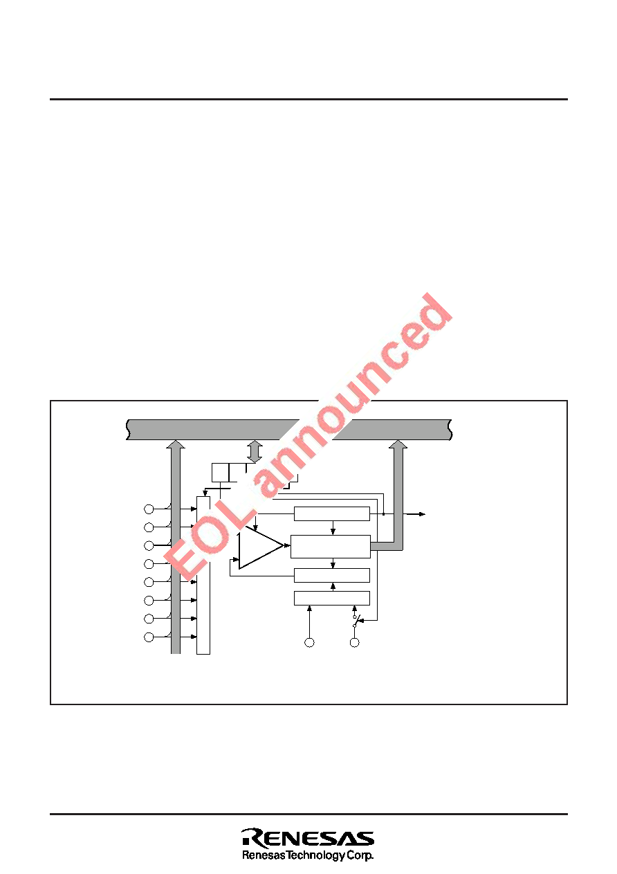
Figure 11 shows a block diagram of the A-D conversion circuit.
Conversion is automatically carried out once started by the pro-
gram.
There are eight analog input pins which are shared with P20 to
P27 of port P2 (Only P20 to P23 4-bit for 7470 group. Which ana-
log inputs are to be A-D converted is specified by using bit 2 to bit
0 in the A-D control register (address 00D916). Pins for inputs to
be A-D converted must be set for input by setting the direction reg-
ister bit to “0”. Bit 3 in the A-D control register is an A-D conversion
end bit. This is “0” during A-D conversion; it is set to “1” when the
conversion is terminated. Therefore, it is possible to know whether
A-D conversion is terminated by checking this bit. Bit 4 in the A-D
control register is a VREF connection selection bit.
During A-D conversion, this bit must be set “1” for the ladder resis-
tor and VREF pin to be connected; after the A-D conversion is
terminated, this bit can be reset to “0” to separate the ladder resis-
tor from the VREF pin. In this way, power consumption in the ladder
resistor can be suppressed while no A-D conversion is performed.
Figure 13 shows the relationship between the contents of A-D
control register and the selected input pins.
The A-D conversion register (address 00DA16) contains informa-
tion on the results of conversion, so that it is possible to know the
results of conversion by reading the contents of this register.
The following explains the procedure to execute A-D conversion.
First, set values to bit 2 to bit 0 in the A-D control register to select
the pins that you want to execute A-D conversion. Next, clear the
A-D conversion end bit to “0”.
When the above is done, A-D conversion is initiated. The A-D con-
version is completed after an elapse of 50 machine cycles
(12.5
s when f(XIN)= 8 MHz), the A-D conversion end bit is set to
“1”, and the interrupt request bit is set to “1”. The results of conver-
sion are contained in the A-D conversion register.
Fig. 11 A-D converter circuit
Comparator
A-D control circuit
Switch tree
Ladder resistor
A-D conversion completion
interrupt request
VSS (Note 1)
VREF
1 : AVSS for M37471M2/M4/M8/E4/E8-XXXFP
2 : 7470 group does not have P2 4/IN4 to P27/IN7 pins.
P20/IN0
P21/IN1
P22/IN2
P23/IN3
P24/IN4
P25/IN5
P26/IN6
P27/IN7
Data bus
A-D control register
(Address 00D916)
bit 4
Channel
selector
Notes
bit 0
A-D conversion register
(Address 00DA16)
相關(guān)PDF資料 |
PDF描述 |
|---|---|
| M37470M8-XXXSP | 8-BIT, MROM, 8 MHz, MICROCONTROLLER, PDIP32 |
| M37470E8-XXXSP | 8-BIT, OTPROM, 8 MHz, MICROCONTROLLER, PDIP32 |
| M37470M2-XXXSP | 8-BIT, MROM, 8 MHz, MICROCONTROLLER, PDIP32 |
| M37471E8-XXXFP | 8-BIT, OTPROM, 8 MHz, MICROCONTROLLER, PQFP56 |
| M37471M2-XXXSP | 8-BIT, MROM, 8 MHz, MICROCONTROLLER, PDIP42 |
相關(guān)代理商/技術(shù)參數(shù) |
參數(shù)描述 |
|---|---|
| M37471E4-XXXSP | 制造商:MITSUBISHI 制造商全稱:Mitsubishi Electric Semiconductor 功能描述:SINGLE-CHIP 8-BIT CMOS MICROCOMPUTER |
| M37471E8SS | 制造商:MITSUBISHI 制造商全稱:Mitsubishi Electric Semiconductor 功能描述:SINGLE-CHIP 8-BIT CMOS MICROCOMPUTER |
| M37471E8-XXXFP | 制造商:MITSUBISHI 制造商全稱:Mitsubishi Electric Semiconductor 功能描述:SINGLE-CHIP 8-BIT CMOS MICROCOMPUTER |
| M37471E8-XXXSP | 制造商:MITSUBISHI 制造商全稱:Mitsubishi Electric Semiconductor 功能描述:SINGLE-CHIP 8-BIT CMOS MICROCOMPUTER |
| M37471M2 | 制造商:MITSUBISHI 制造商全稱:Mitsubishi Electric Semiconductor 功能描述:SINGLE-CHIP 8-BIT CMOS MICROCOMPUTER |
發(fā)布緊急采購,3分鐘左右您將得到回復(fù)。