- 您現在的位置:買賣IC網 > PDF目錄45030 > M37225M6-XXXSP 8-BIT, MROM, 8.1 MHz, MICROCONTROLLER, PDIP42 PDF資料下載
參數資料
| 型號: | M37225M6-XXXSP |
| 元件分類: | 微控制器/微處理器 |
| 英文描述: | 8-BIT, MROM, 8.1 MHz, MICROCONTROLLER, PDIP42 |
| 封裝: | 0.600 INCH, PLASTIC, SDIP-42 |
| 文件頁數: | 93/126頁 |
| 文件大小: | 1486K |
| 代理商: | M37225M6-XXXSP |
第1頁第2頁第3頁第4頁第5頁第6頁第7頁第8頁第9頁第10頁第11頁第12頁第13頁第14頁第15頁第16頁第17頁第18頁第19頁第20頁第21頁第22頁第23頁第24頁第25頁第26頁第27頁第28頁第29頁第30頁第31頁第32頁第33頁第34頁第35頁第36頁第37頁第38頁第39頁第40頁第41頁第42頁第43頁第44頁第45頁第46頁第47頁第48頁第49頁第50頁第51頁第52頁第53頁第54頁第55頁第56頁第57頁第58頁第59頁第60頁第61頁第62頁第63頁第64頁第65頁第66頁第67頁第68頁第69頁第70頁第71頁第72頁第73頁第74頁第75頁第76頁第77頁第78頁第79頁第80頁第81頁第82頁第83頁第84頁第85頁第86頁第87頁第88頁第89頁第90頁第91頁第92頁當前第93頁第94頁第95頁第96頁第97頁第98頁第99頁第100頁第101頁第102頁第103頁第104頁第105頁第106頁第107頁第108頁第109頁第110頁第111頁第112頁第113頁第114頁第115頁第116頁第117頁第118頁第119頁第120頁第121頁第122頁第123頁第124頁第125頁第126頁
69
SINGLE-CHIP 8-BIT CMOS MICROCOMPUTER for VOLTAGE SYNTHESIZER
with ON-SCREEN DISPLAY CONTROLLER
M37225M6/M8/MA/MC–XXXSP
M37225ECSP
MITSUBISHI MICROCOMPUTERS
Rev. 1.0
(4) Character color
Character colors are specified by RA1 to RA3 of OSD RAM.
Color data are set by color register i (CO1 to CO8: addresses 00E616
to 00E916, 00EC16 to 00EF16) in advance, and 8 kinds of color regis-
ter i are specified by color codes.
(5) Character background color
Character background are specified by color register i as same as
character color.
Note : The character background is displayed in the following part:
(character display area) – (character font) — (border) – (BUTTON display area)
Accordingly, the character background color and the color signal for
these sections cannot be mixed.
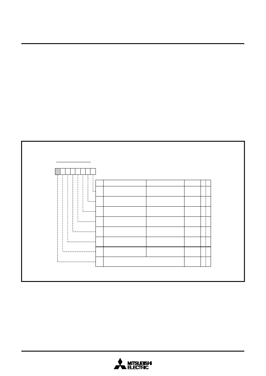
Fig. 8.10.19 Color register i (i = 1 to 8)
(6) OUT1, OUT2 signals
OUT1 signal is used to erase a back ground TV image. The output
waveform of OUT1 signal is controlled by combining the following
bits; the display mode selection bits (bits 0 to 2 of the block i control
register), the border type selection bit (bit 1 of the OSD control regis-
ter), and the OUT1 output control bit (bit 6 of color register i).
Figure 8.10.20 and 8.10.21 shows the output example of R, G, B,
and OUT1.
OUT2 signal is used to change the luminance of a background TV
image. The output waveform of OUT2 signal is blank output and is
controlled per character unit by RA6 of OSD RAM.
b7 b6 b5 b4 b3 b2 b1 b0
Color register i (CO1 to CO8) (i=1 to 8) [Addresses 00E616 to 00E916, 00EC16 to 00EF16]
B
Name
Functions
After reset
R W
Color Register i
0
Indeterminate R W
1
G signal output selection
bit (COi1)
0: No output
1: Output
R W
2
B signal output selection
bit (COi2)
0: No output
1: Output
R W
3
R signal output (background)
selection bit (COi3)
0: No output
1: Output
R W
4
G signal output (background)
selection bit (COi4)
0: No output
1: Output
R W
5
B signal output (background)
selection bit (COi5)
0: No output
1: Output
R W
6
OUT1 output control bit
(COi6)
0: Character output
1: Blank output
R W
7
0
R —
R signal output selection
bit (COi0)
0: No output
1: Output
Nothing is assined. This bit is a write disable bit.
When this bit is read out, the value is “0.”
Indeterminate
相關PDF資料 |
PDF描述 |
|---|---|
| M37225MA-XXXSP | 8-BIT, MROM, 8.1 MHz, MICROCONTROLLER, PDIP42 |
| M37225MC-XXXSP | 8-BIT, MROM, 8.1 MHz, MICROCONTROLLER, PDIP42 |
| M37225ECSP | 8-BIT, OTPROM, 8.1 MHz, MICROCONTROLLER, PDIP42 |
| M37250M6-XXXSP | 8-BIT, MROM, 4 MHz, MICROCONTROLLER, PDIP64 |
| M37260E6FP | 8-BIT, OTPROM, 8 MHz, MICROCONTROLLER, PQFP64 |
相關代理商/技術參數 |
參數描述 |
|---|---|
| M37225M8 | 制造商:RENESAS 制造商全稱:Renesas Technology Corp 功能描述:SNGLE-CHIP 8-BIT CMOS MICROCOMPUTER for VOLTAGE SYNTHESIZER with ON-SCREEN DISPLAY CONTROLLER |
| M37225MA | 制造商:RENESAS 制造商全稱:Renesas Technology Corp 功能描述:SNGLE-CHIP 8-BIT CMOS MICROCOMPUTER for VOLTAGE SYNTHESIZER with ON-SCREEN DISPLAY CONTROLLER |
| M372429100 | 制造商:ITW Switches 功能描述:IN-RUSH |
| M372429200 | 制造商:ITW Switches 功能描述:IN-RUSH |
| M372499100 | 制造商:ITW Switches 功能描述:IN-RUSH |
發(fā)布緊急采購,3分鐘左右您將得到回復。