- 您現(xiàn)在的位置:買賣IC網(wǎng) > PDF目錄370841 > M37221M6 (Mitsubishi Electric Corporation) Single Chip 8 Bits Microcomputer(8位單片機) PDF資料下載
參數(shù)資料
| 型號: | M37221M6 |
| 廠商: | Mitsubishi Electric Corporation |
| 英文描述: | Single Chip 8 Bits Microcomputer(8位單片機) |
| 中文描述: | 單芯片8位單片機(8位單片機) |
| 文件頁數(shù): | 24/61頁 |
| 文件大?。?/td> | 1386K |
| 代理商: | M37221M6 |
第1頁第2頁第3頁第4頁第5頁第6頁第7頁第8頁第9頁第10頁第11頁第12頁第13頁第14頁第15頁第16頁第17頁第18頁第19頁第20頁第21頁第22頁第23頁當(dāng)前第24頁第25頁第26頁第27頁第28頁第29頁第30頁第31頁第32頁第33頁第34頁第35頁第36頁第37頁第38頁第39頁第40頁第41頁第42頁第43頁第44頁第45頁第46頁第47頁第48頁第49頁第50頁第51頁第52頁第53頁第54頁第55頁第56頁第57頁第58頁第59頁第60頁第61頁

MITSUBISHI MICROCOMPUTERS
M37221M6-XXXSP
SINGLE-CHIP 8-BIT CMOS MICROCOMPUTER for VOLTAGE SYNTHESIZER
with ON-SCREEN DISPLAY CONTROLLER
24
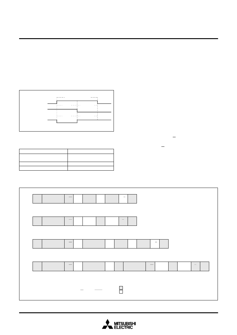
Fig. 21. START condition/STOP condition detecting timing diagram
Table 5. START condition/STOP condition detecting conditions
(8) START/STOP Condition Detecting Condi-
tions
The START/STOP condition detecting conditions are shown in Fig-
ure 21 and Table 5. Only when the 3 conditions of Table 5 are satis-
fied, a START/STOP condition can be detected.
Note:
When a STOP condition is detected in the slave mode
(MST = 0), an interrupt request signal “IICIRQ” occurs to the
CPU.
Standard clock mode
6.5
μ
s (26 cycles) < SCL release
time
3.25
μ
s (13 cycles) < Setup time
3.25
μ
s (13 cycles) < Hold time
High-speed clock mode
1.0
μ
s (4 cycles) < SCL release
time
0.5
μ
s (2 cycles) < Setup time
0.5
μ
s (2 cycles) < Hold time
Note:
Absolute time at
φ
= 4 MHz. The value in parentheses de-
notes the number of
φ
cycles.
(9) Address Data Communication
There are two address data communication formats, namely, 7-bit
addressing format and 10-bit addressing format. The respective ad-
dress communication formats is described below.
7-bit addressing format
To meet the 7-bit addressing format, set the 10BIT SAD bit of the
I
2
C control register (address 00DA
16
) to “0.” The first 7-bit address
data transmitted from the master is compared with the high-order
7-bit slave address stored in the I
2
C address register (address
00D8
16
). At the time of this comparison, address comparison of
the RBW bit of the I
2
C address register (address 00D8
16
) is not
made. For the data transmission format when the 7-bit addressing
format is selected, refer to Figure 22, (1) and (2).
10-bit addressing format
To meet the 10-bit addressing format, set the 10BIT SAD bit of the
I
2
C control register (address 00DA
16
) to “1.” An address compari-
son is made between the first-byte address data transmitted from
the master and the 7-bit slave address stored in the I
2
C address
register (address 00D8
16
). At the time of this comparison, an ad-
dress comparison between the RBW bit of the I
2
C address regis-
ter (address 00D8
16
) and the R/W bit which is the last bit of the
address data transmitted from the master is made. In the 10-bit
addressing mode, the R/W bit which is the last bit of the address
data not only specifies the direction of communication for control
data but also is processed as an address data bit.
Fig. 22. Address data communication format
AA
Hold time
AA
Hold time
Setup
time
SCL
SDA
(START condition)
SDA
(STOP condition)
SCL release time
Setup
time
S
Slave address
A
Data
A
Data
A/A
P
R/W
7 bits
“0”
1 to 8 bits
1 to 8 bits
S
Slave address
A
Data
A
Data
A
P
7 bits
“1”
1 to 8 bits
1 to 8 bits
(1) A master-transmitter transmits data to a slave-receiver
S
Slave address
1st 7 bits
A
A
Data
7 bits
“0”
8 bits
1 to 8 bits
(2) A master-receiver receives data from a slave-transmitter
Slave address
2nd byte
A
Data
A/A
P
1 to 8 bits
S
Slave address
1st 7 bits
A
A
7 bits
“0”
8 bits
7 bits
(3) A master-transmitter transmits data to a slave-receiver with a 10-bit address
Slave address
2nd byte
Data
1 to 8 bits
Sr
Slave address
1st 7 bits
A
Data
A
P
1 to 8 bits
“1”
(4) A master-receiver receives data from a slave-transmitter with a 10-bit address
S : START condition
A : ACK bit
Sr : Restart condition
P : STOP condition
R/W : Read/Write bit
From master to slave
From slave to master
A
R/W
R/W
R/W
R/W
相關(guān)PDF資料 |
PDF描述 |
|---|---|
| M37221 | SINGLE-CHIP 8-BIT CMOS MICROCOMPUTER for VOLTAGE SYNTHESIZER with ON-SCREEN DISPLAY CONTROLLER |
| M37221EFSP | SINGLE-CHIP 8-BIT CMOS MICROCOMPUTER for VOLTAGE SYNTHESIZER with ON-SCREEN DISPLAY CONTROLLER |
| M37266ME-XXXSP | SINGLE-CHIP 8-BIT CMOS MICROCOMPUTER with CLOSED CAPTION DECODER and ON-SCREEN DISPLAY CONTROLLER |
| M37266EESP | SINGLE-CHIP 8-BIT CMOS MICROCOMPUTER with CLOSED CAPTION DECODER and ON-SCREEN DISPLAY CONTROLLER |
| M37266EE-XXXSP | SINGLE-CHIP 8-BIT CMOS MICROCOMPUTER with CLOSED CAPTION DECODER and ON-SCREEN DISPLAY CONTROLLER |
相關(guān)代理商/技術(shù)參數(shù) |
參數(shù)描述 |
|---|---|
| M37221M6_03 | 制造商:RENESAS 制造商全稱:Renesas Technology Corp 功能描述:SINGLE-CHIP 8-BIT CMOS MICROCOMPUTER for VOLTAGE SYNTHESIZER with ON-SCREEN DISPLAY CONTROLLER |
| M37221M6-054SP | 制造商:MITSUBISHI 制造商全稱:Mitsubishi Electric Semiconductor 功能描述:SINGLE-CHIP 8-BIT CMOS MICROCOMPUTER for VOLTAGE SYNTHESIZER |
| M37221M6-079SP | 制造商:MITSUBISHI 制造商全稱:Mitsubishi Electric Semiconductor 功能描述:SINGLE-CHIP 8-BIT CMOS MICROCOMPUTER for VOLTAGE SYNTHESIZER |
| M37221M6-286SP | 制造商:MITSUBISHI 制造商全稱:Mitsubishi Electric Semiconductor 功能描述:SINGLE-CHIP 8-BIT CMOS MICROCOMPUTER for VOLTAGE SYNTHESIZER |
| M37221M6H | 制造商:RENESAS 制造商全稱:Renesas Technology Corp 功能描述:SINGLE-CHIP 8-BIT CMOS MICROCOMPUTER for VOLTAGE SYNTHESIZER with ON-SCREEN DISPLAY CONTROLLER |
發(fā)布緊急采購,3分鐘左右您將得到回復(fù)。