- 您現(xiàn)在的位置:買賣IC網(wǎng) > PDF目錄383296 > M37220M3-157SP (Mitsubishi Electric Corporation) SINGLE-CHIP 8-BIT CMOS MICROCOMPUTER for VOLTAGE SYNTHESIZER with ON-SCREEN DISPLAY CONTROLLER PDF資料下載
參數(shù)資料
| 型號: | M37220M3-157SP |
| 廠商: | Mitsubishi Electric Corporation |
| 英文描述: | SINGLE-CHIP 8-BIT CMOS MICROCOMPUTER for VOLTAGE SYNTHESIZER with ON-SCREEN DISPLAY CONTROLLER |
| 中文描述: | 單芯片8位CMOS微機電壓合成與屏幕顯示控制器 |
| 文件頁數(shù): | 4/53頁 |
| 文件大小: | 1281K |
| 代理商: | M37220M3-157SP |
第1頁第2頁第3頁當(dāng)前第4頁第5頁第6頁第7頁第8頁第9頁第10頁第11頁第12頁第13頁第14頁第15頁第16頁第17頁第18頁第19頁第20頁第21頁第22頁第23頁第24頁第25頁第26頁第27頁第28頁第29頁第30頁第31頁第32頁第33頁第34頁第35頁第36頁第37頁第38頁第39頁第40頁第41頁第42頁第43頁第44頁第45頁第46頁第47頁第48頁第49頁第50頁第51頁第52頁第53頁
MITSUBISHI MICROCOMPUTERS
M37220M3-XXXSP
SINGLE-CHIP 8-BIT CMOS MICROCOMPUTER for VOLTAGE SYNTHESIZER
with ON-SCREEN DISPLAY CONTROLLER
4
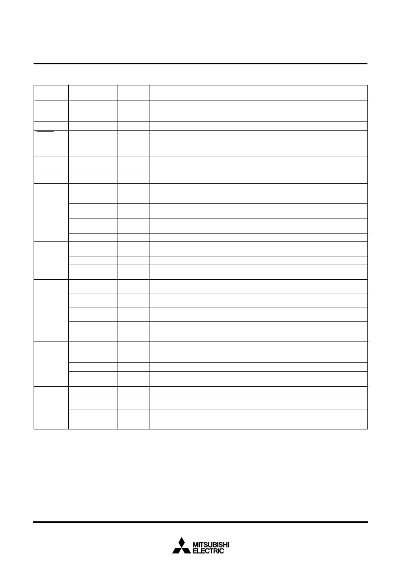
PIN DESCRIPTION
Pin
Input/
Output
Name
V
CC,
V
SS
CNV
SS
RESET
X
IN
X
OUT
P0
0
/PWM0–
P0
5
/PWM5,
P0
6
/INT2/
A-D4,
P0
7
/INT1
P1
0
–P1
4
,
P1
5
/A-D1
INT3,
P1
6
/A-D2,
P1
7
/A-D3
P2
0
/S
CLK
,
P2
1
/S
OUT
,
P2
2
/S
IN
,
P2
3
/TIM3,
P2
4
/TIM2,
P2
5
–P2
7
P3
0
/A-D5/
DA1,
P3
1
/A-D6/
DA2,
P3
2
P3
3
/OSC1,
P3
4
/OSC2
Apply voltage of 5 V
±
10 % (typical) to V
CC
, and 0 V to V
SS
.
This is connected to V
SS
.
To enter the reset state, the reset input pin must be kept at a “L” for 2
μ
s or more (under
normal V
CC
conditions).
If more time is needed for the quartz-crystal oscillator to stabilize, this “L” condition should
be maintained for the required time.
This chip has an internal clock generating circuit. To control generating frequency, an
external ceramic resonator or a quartz-crystal oscillator is connected between pins X
IN
and
X
OUT
. If an external clock is used, the clock source should be connected to the X
IN
pin and
the X
OUT
pin should be left open.
Port P0 is an 8-bit I/O port with direction register allowing each I/O bit to be individually
programmed as input or output. At reset, this port is set to input mode. The output structure
is N-channel open-drain output. The note out of this Table gives a full of port P0 function.
Pins P0
0
–P0
5
are also used as PWM output pins PWM0–PWM5 respectively.The output
structure is N-channel open-drain output.
Pins P0
6
, P0
7
are also used as external interrupt input pins INT2, INT1 respectively.
Pins P0
6
is also used as an analog interrupt input pin A-D4.
Port P1 is an 8-bit I/O port and has basically the same functions as port P0. The output
structure is CMOS output.
Pins P1
5
–P1
7
are also used as an analog input pins A-D1 to A-D3.
Pin P1
5
is also used as an external interrupt input pins INT3.
Port P2 is an 8-bit I/O port and has basically the same functions as port P0. The output
structure is CMOS output.
Pins P2
3
, P2
4
is also used an external clock input pins TIM3, TIM2 respectively.
Pins P2
1
, P2
2
are also used serial I/O data input/output pins S
OUT
, S
IN
respectively. The
output structure is N-channel open-drain output.
Pin P2
0
is also used serial I/O syncronizing clock input/output pin S
CLK
. The output struc-
ture is N-channel open-drain output.
Ports P3
0
–P3
2
are a 3-bit I/O port and have basically the same functions as port P0. Either
CMOS output or N-channel open-drain output structure can be selected as the ports P3
0
and P3
1
. The output structure of port P3
2
is N-channel open-drain output.
Pins P3
0
, P3
1
are also used as analog input pins A-D5, A-D6 respectively.
Pins P3
0
, P3
1
are also used as D-A conversion output pins DA1, DA2 respectively.
Ports P3
3
, P3
4
are a 2-bit input port.
Pin P3
3
is also used as CRT display clock input pin OSC1.
Pin P3
4
is also used as CRT display clock output pin OSC2.The output structure is CMOS
output.
Input
Input
Output
I/O
Output
Input
Input
I/O
Input
Input
I/O
Input
I/O
I/O
I/O
Input
Output
Input
Input
Output
Power source
CNV
SS
Reset input
Clock input
Clock output
I/O port P0
PWM output
External interrupt
input
Analog input
I/O port P1
Analog input
External interrupt
input
I/O port P2
External clock
input
Serial I/O data
input/output
Serial I/O synchro-
nizing clock input/
output
I/O port P3
Analog input
D-A conversion
output
Input port P3
Clock input for
CRT display
Clock output for
CRT display
Functions
相關(guān)PDF資料 |
PDF描述 |
|---|---|
| M37220M3-160SP | SINGLE-CHIP 8-BIT CMOS MICROCOMPUTER for VOLTAGE SYNTHESIZER with ON-SCREEN DISPLAY CONTROLLER |
| M37220M3-167SP | SINGLE-CHIP 8-BIT CMOS MICROCOMPUTER for VOLTAGE SYNTHESIZER with ON-SCREEN DISPLAY CONTROLLER |
| M37273EF8SP | SINGLE-CHIP 8-BIT CMOS MICROCOMPUTER with CLOSED CAPTION DECODER and ON-SCREEN DISPLAY CONTROLLER |
| M37273E8SP | Single Chip 8 Bits Microcomputer(8位單片機) |
| M37273EFSP | Single Chip 8 Bits Microcomputer(8位單片機) |
相關(guān)代理商/技術(shù)參數(shù) |
參數(shù)描述 |
|---|---|
| M37220M3-160SP | 制造商:MITSUBISHI 制造商全稱:Mitsubishi Electric Semiconductor 功能描述:SINGLE-CHIP 8-BIT CMOS MICROCOMPUTER for VOLTAGE SYNTHESIZER with ON-SCREEN DISPLAY CONTROLLER |
| M37220M3-167SP | 制造商:MITSUBISHI 制造商全稱:Mitsubishi Electric Semiconductor 功能描述:SINGLE-CHIP 8-BIT CMOS MICROCOMPUTER for VOLTAGE SYNTHESIZER with ON-SCREEN DISPLAY CONTROLLER |
| M37220M3-XXXSP | 制造商:RENESAS 制造商全稱:Renesas Technology Corp 功能描述:SINGLE-CHIP 8-BIT CMOS MICROCOMPUTER for VOLTAGE SYNTHESIZER with ON-SCREEN DISPLAY CONTROLLER |
| M37221 | 制造商:MITSUBISHI 制造商全稱:Mitsubishi Electric Semiconductor 功能描述:SINGLE-CHIP 8-BIT CMOS MICROCOMPUTER for VOLTAGE SYNTHESIZER |
| M37221EAFP | 制造商:RENESAS 制造商全稱:Renesas Technology Corp 功能描述:SINGLE-CHIP 8-BIT CMOS MICROCOMPUTER for VOLTAGE SYNTHESIZER with ON-SCREEN DISPLAY CONTROLLER |
發(fā)布緊急采購,3分鐘左右您將得到回復(fù)。